Search for articles:
Y. Zhang , M. Turghun
Corresponding authors:
Received: 2017-09-19
Revised: 2017-10-31
Online: 2018-06-10
Copyright: 2018 Editorial board of Acta Metallurgica Sinica(English Letters) Copyright reserved, Editorial board of Acta Metallurgica Sinica(English Letters)
More
Abstract
FeGa thin film has been deposited on (100)-oriented GaAs and (001)-oriented Si substrates with different film thicknesses and laser energy densities at room temperature by pulsed laser deposition system. Materials structure and static magnetic of FeGa film have great changes depending on the substrate and energy density of pulsed laser. X-ray diffraction reveals the presence of first-order order-disorder structure of D03-ordered grain phase and disordered bcc A2 structure on GaAs substrate. The coercivity and remanence of FeGa film on GaAs substrate ratio show a regular dependence on the thickness and energy densities. However, film on Si substrate did not exhibit structure change, which can be attributed to a large lattice mismatch between FeGa and Si.
Keywords:
With the rapid development of electronic computer and information technology, highly sensitive magnetic film sensor has attracted widespread attention in recent years [1]. Magnetoelectric (ME) coupling sensor as a kind of thin film sensor has been reported, and using magnetoelectric coupling effect to change magnetization reversal mechanism has become a hot research topic [2, 3]. Normally, the magnetic components in ME systems should have excellent characteristics of soft magnetic and large magnetostriction [4, 5]. But traditional ME magnetic materials can hardly have the both characters, such as TbDyFe, CoFeSiB, etc. [6, 7]. FeGa thin films as a function of new type of ferromagnetic materials are an exciting material due to its large magnetostriction constant, high saturation magnetization and low coercivity [8]. Several kinds of preparation methods have been reported to fabricate FeGa thin film under room temperature, including electro-deposition [9], molecular beam epitaxy [10], ion beam sputtering [11] and magnetic sputtering [12]. On the one hand, in order to enhance the magnetostrictive property, previous studies have shown that FeGa alloys have a variety of phases, including A2, B2, D03, L12, which is very sensitive to the detail of its production. For example, A2, D03, L12 coexisted in rapidly quenched polycrystalline FeGa film [13]; a mixture of A2 and D03 has been observed in arc-melted FeGa alloys [14]; A2-textured FeGa film has been fabricated using molecular beam epitaxy [15]. On the other hand, the static magnetic property (especially the magnetostriction) of FeGa film can be influenced by its elemental constituent, which is mainly dependent on the film fabrication [16]. However, pulsed laser deposition (PLD) as a kind of widely used high-quality thin film preparation process [17, 18], which can keep the atomic ratio accurate, has not yet been reported in the preparation of iron gallium. In this study, we fabricated FeGa film on (100)-oriented GaAs and (001)-oriented Si substrates using pulsed laser deposition successfully and investigated influences of the substrate, thickness and laser energy density on the structure and magnetic properties of FeGa thin film.
FeGa film was deposited on (100)-oriented GaAs and (001)-oriented Si single-crystal substrates (purchased from Hefei Kejing materials technology Co., LTD, Hefei, China) by pulse laser deposition system (high-power KrF excimer laser, COMPexProTM 201 F, λ = 248 nm) with the base pressure below 6 × 10⁻⁷ Torr. All the samples were fabricated at room temperature. The FeGa alloy target (atom ratio of Fe/Ga is 83:17) was commercially available (purchased from Zhongnuo New Materials Co., LTD, Beijing, China). The purity and the diameter of the target were 99.99% and 1 in., respectively. The substrate area of GaAs and Si was 1 × 1 cm2. Prior to deposition, the GaAs and Si substrates were cleaned by acetone, methanol and deionized water for 5 min, respectively. Laser energy density could be tuned from 1.00 to 2.00 J/cm2, and frequency was kept constant at 5 Hz. The films with different thicknesses were fabricated using 1.00 J/cm2, and the laser pulse duration was 10-40 min. The distance from the substrate to the target was about 5 cm. During deposition, the substrate was rotated at a constant speed of 5.9 rpm and target was rotated at a constant speed of 7.3 rpm to obtain uniformity in thickness and composition.
Atomic force microscope (AFM, MFP-3D, Asylum Research, USA) was carried out to investigate the surface topography of the samples. The surface and interface morphologies of the film were determined by using a field emission scanning electron microscope (FESEM, S-4800, Hitachi, Tokyo, Japan) equipped with an energy-dispersive X-ray spectrometer (EDS). Inductively couple plasma (ICP) atomic emission spectrometry was also used to confirm the chemical composition. Film thickness was determined by surface profilometer measurements. X-ray diffraction (XRD, D8 Focus, Bruker AXS, Karlsruhe, Germany) patterns were recorded by analytical diffractometer using Cu-Kα radiation with λ¼ = 0.15418 nm. Magnetization measurements were carried out by applying a magnetic field up to 5 KOe under in-plane direction at room temperature using vibrating sample magnetometer (VSM, 7404, Lakeshore, Westerville, OH, USA).
Figure 1a-e shows the typical SEM images of prepared FeGa films on (100)-GaAs and (001)-Si substrate, respectively. The grains are very fine for the film deposition. It can hardly find any defects on the surface of FeGa film, especially on the GaAs substrate, as shown in Fig. 1a. Some small impurities can faintly be seen on the surface of FeGa film when the film was fabricated on Si substrate, as shown in Fig. 1d. From the cross-sectional view of the film, we can find the FeGa film is completely coated on the substrate, which has a uniform thickness, as shown Fig. 1b, e. The thickness results from SEM images are well according to the results measured by profilometer, which could be found in supporting information Fig. 2. The chemical composition of FeGa has been measured by EDS, which remained the same as the laser energy density changes (Table 1). AFM images of FeGa films deposited on GaAs and Si substrate obtained over a scan area of 2 μm × 2 μm by AFM are shown in Fig. 1c, f. The RMS roughness of FeGa film on GaAs substrate is 1.887 nm, which is much better than the film on Si substrate (3.582 nm). It indicates that GaAs substrate is more suitable than Si substrate for FeGa film-oriented growing.
Fig. 1 Typical SEM images of FeGa film on GaAs and Si, respectively. a Surface topography on GaAs; b cross-sectional image on GaAs; c AFM 3D image; d surface topography on Si, e cross-sectional image on Si; f AFM 3D image
Fig. 2 Thicknesses of FeGa thin film on GaAs and Si substrate with different deposition time and laser energy densities
Table 1 Chemical composition of FeGa film measured by EDS and ICP, respectively
| Laser energy density | |||||
|---|---|---|---|---|---|
| 1.00 J cm-2 | 1.33 J cm-2 | 1.67 J cm-2 | 2.00 J cm-2 | ||
| Fe (at.%) | 86.57 | 87.70 | 87.81 | 87.83 | Measured by EDS |
| Ga (at.%) | 13.43 | 12.30 | 12.19 | 12.17 | |
| Fe (at.%) | - | - | 87.83 | 88.10 | Measured by ICP |
| Ga (at.%) | - | - | 12.17 | 11.90 | |
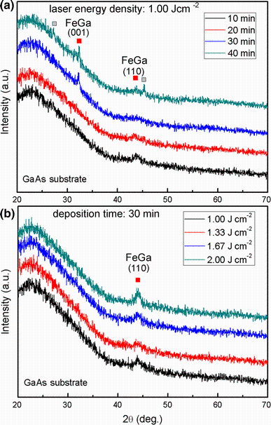
Typical XRD patterns of FeGa thin films deposited on GaAs substrate at different deposition time and laser energy densities are shown in Fig. 3. It is observed that a tiny diffraction peak appears at 2θ = 44° when the film deposition time is 10 and 20 min, but another diffraction peak appears at 2θ = 31.7° when the film deposition time are 30 and 40 min. The diffraction peak (2θ = 31.7°) is corresponding to (001) direction that D03-ordered grain phase in the bcc α-Fe crystal and the diffraction peak (2θ = 44°) is corresponding to (110) growth direction of bcc α-Fe crystal (A2) structure [19, 20]. However, the diffraction peak appears at θ = 44° for all of the samples, which is corresponding to (110) growth direction that bcc α-Fe crystal (A2) structure when changing the laser energy density as shown in Fig. 3b. The results of the XRD indicate that: (1) the FeGa film growth tends to the bcc α-Fe crystal (110) direction under room temperature on GaAs substrate, and (001) D03-ordered grain phase can be induced by a proper thickness; (2) the laser energy density cannot change the texture of FeGa film; (3) the film shows obvious nanocrystalline property and amorphous trend due to broad peak and weak intensity.
Fig. 3 XRD patterns of FeGa films on GaAs substrate with different deposition time a laser energy densities b
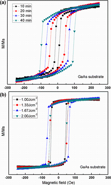
The hysteresis loops of FeGa film under different deposition time and laser energy densities on GaAs substrate, which are measured in an in-plane external magnetic field, are shown in Fig. 4. The soft magnetic properties could be observed in all the samples under different deposition time. The coercivity of FeGa film increases with the deposition time. The maximum and the minimum coercivities of FeGa film are 97 and 12 Oe when the deposition time is 40 and 10 min, respectively. The remanence ratio Mr/Ms of FeGa film on GaAs substrate is from 0.90 to 0.7 along with the increase in deposition time, as shown in Fig. 4a. Obviously, with increasing the deposition time, the magnetic coercivity and the remanence ratio both turn large. The thickness of the film increases linearly with the deposition time (Fig. 2). The change in magnetic properties could be attributed to the formation of nanocrystalline or amorphous during the film growth [21, 22], especially when the deposition time is short. Because of an instantaneous high-temperature process of PLD, a mixture phase of A2, D03 could be induced, which is like arc-melted fabrication. With the emergence and enhancement of D03 phase, the hysteresis loops of FeGa film have a bigger coercivity and a better squareness ratio, which means that the FeGa film has a larger magnetocrystalline anisotropy. These results are well compliant with the XRD data.
Fig. 4 VSM magnetic hysteresis loops of FeGa films on GaAs substrate with different deposition time a laser energy densities b
When the FeGa film is deposited on GaAs substrate with different laser energy densities, the coercivity of FeGa film firstly increases and then decreases, and the remanence ratio shows the opposite trend. On the one hand, from the supporting information Fig. 2, we can find that the thickness of the FeGa film has a nonlinear relationship with the laser energy density, but it has a similar tendency with the coercivity. On the other hand, it is not difficult to find that the soft magnetic properties have a little change with different laser energy densities. The maximum coercivity and minimum remanence ratio appear when the laser energy density is 1.67 J/cm2, which signifies a weak soft magnetic property. A large laser energy density might take the non-uniform distribution of Fe, Ga elements. So in order to keep a good magnetic property, a proper laser density should be necessary.
Figure 5a, b shows the X-ray diffraction patterns of the FeGa thin films deposited on Si substrate at different deposition time and laser energy density, respectively. Compared with Fig. 3, FeGa film deposited on Si substrate shows obvious amorphous property. Rather than the FeGa film deposited on the GaAs substrate, the film on Si substrate does not show the (001)-directed D03-ordered grain phase. This is mainly due to the large lattice mismatch between Si and FeGa.
Fig. 5 XRD patterns of FeGa films on Si substrate with different deposition time a laser energy densities b
The magnetization hysteresis loops of FeGa thin film deposited on Si substrate at different deposition time and laser energy densities are shown in Fig. 6a, b, respectively. The coercivity of FeGa film on (001) Si substrate increases from 14 to 108 Oe, but the remanence ratio only shows a tiny and mild rise with the increase in deposition time. From the X-ray patterns, we can find that the film keeps an obvious non-crystallizing, irrespective of the increase in deposition time or laser energy density. The FeGa film has a very good soft magnetic property when the laser energy changes. The enlargement of the coercivity and the remanence ratio could be attributed to the surface roughness and the composition non-uniformity.
Fig. 6 VSM magnetic hysteresis loops of FeGa films on Si substrate with different deposition time a laser energy densities b
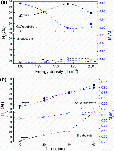
Figure 7 shows the details of magnetic parameter of FeGa film on (100)-oriented GaAs and (001)-oriented Si substrates. On the one hand, as shown in Fig. 7a, with the increase in deposition time, the coercivity and the remanence ratio of the former have a linear growth trend; but latter can only keep a rising tendency. On the other hand, the coercivity and the remanence of FeGa film on (100)-oriented GaAs show cosine and sine curves, respectively, but the magnetic property is almost invariant when the film is deposited on Si substrate. So in practical application, we can obtain an excellent soft magnetic FeGa film if it is fabricated on (001)-oriented Si substrate and a well magnetostrictive FeGa film if it is fabricated on (100)-oriented GaAs substrate, which should have the (001)-directed D03-ordered grain phase.
Fig. 7 Details of Hc and Mr/Ms of FeGa film fabricated on different substrates with the increase in energy density a deposition time b
4 Conclusion
FeGa thin films have been successfully prepared by PLD on (100)-oriented GaAs and (100)-oriented Si substrates. FeGa film grown on GaAs shows a changeable structure depending on the fabrication conditions. The D03 gain structure and preferred orientation growth that according to the (001) direction on GaAs substrate have been observed. The coercivity and remanence ratio show a regular dependence on thickness and energy densities. A good soft magnetic property can be kept when the film has been fabricated on Si substrate. The result may provide a fundamental data for FeGa film applied in magnetoelectric sensors.
The authors have declared that no competing interests exist.

 WeChat
/
| 〈 |
|
〉 |


