Search for articles:
Ying-Feng He , Xin-He Zheng
Corresponding authors:
Received: 2019-03-26
Revised: 2019-05-31
Online: 2019-12-10
Copyright: 2019 Editorial board of Acta Metallurgica Sinica(English Letters) Copyright reserved, Editorial board of Acta Metallurgica Sinica(English Letters)
More
Abstract
In this work, the GaN thin films were directly deposited on multilayer graphene (MLG) by plasma-enhanced atomic layer deposition. The deposition was carried out at a low temperature using triethylgallium (TEGa) precursor and Ar/N2/H2 plasma. Chemical properties of the bulk GaN and GaN-graphene interface were analyzed using X-ray photoelectron spectroscopy. The sharp interface between GaN and graphene was verified via X-ray reflectivity and transmission electron microscope. The microstructures and the nucleation behaviors of the GaN grown on graphene have been also studied. The results of grazing incidence X-ray diffraction and Raman spectrum indicate that the as-deposited sample is polycrystalline with wurtzite structure and has a weakly tensile stress. Optical properties of the sample were investigated by photoluminescence (PL) at room temperature. The successful growth of GaN on MLG at a low temperature opens up the possibility of ameliorating the performance of electronic and optical devices based on GaN/graphene heterojunction.
Keywords:
Due to their excellent material properties, III-nitride semiconductors are widely used for optical and electronic devices [1, 2, 3]. Graphene, a two-dimensional material, has already been applied in a great number of fields owing to its outstanding physical properties [4]. The combination of graphene and GaN has been recently considered with the aim to solve some important problems in GaN-based devices. Furthermore, new devices can be created which depends on the combination [5]. To data, some groups studied the integration of graphene with GaN for improving the properties of the GaN-based light emitting diode (LED) [6]. In other research studies, GaN/graphene heterostructure was used for high-power and high-frequency applications [7]. And to make better use of the integration of graphene with GaN, some experimental observations have been reported which reveal the physical properties of the GaN/graphene heterostructure. Tongay et al. studied the thermal stability of graphene/GaN Schottky diodes [8] and rectification at graphene-GaN interface [9]. After that, the contact properties of graphene on GaN were reported by Zhong et al. [10, 11]. And Wang et al. [12] presented a method to improve transport properties of graphene/GaN heterostructure.
The study by Al Balushi et al. [13] has shown that the direct epitaxy of GaN on graphene is difficult owing to the dangling-bond-free surface of graphene. In this context, various methods were utilized to change the surface of graphene aiming at depositing suitable crystalline quality GaN thin films on graphene without damaging the good properties of graphene [14, 15, 16]. However, some devices require the direct deposition of GaN on graphene. The hot electron transistors found on graphene/AlGaN/GaN heterojunction, for instance, need to use GaN as base-collector barrier to achieve optimal performance [16]. This demands the direct deposition of GaN on graphene. Metal organic chemical vapor deposition (MOCVD) and molecular beam epitaxy (MBE) have been employed to reach the goal [17, 18, 19]. All these epitaxial techniques, however, required high deposition temperatures, which is not either consistent with the existing complementary metal-oxide semiconductor technology or suitable for temperature-sensitive substrates. Except for the high growth temperatures, the surface of GaN thin films directly deposited on graphene via MOCVD/MBE is rough which has a bad effect on devices. Atomic layer deposition (ALD) is a promising technique which can deposit smooth, continuous and pinhole-free films on substrates at low temperatures. And thanks to the high reactivity provided by plasma, plasma-enhanced atomic layer (PEALD) offers better material properties compared to thermal ALD [20]. What’s more, the combination of III-nitride nanowires and nanopyramids with graphene has recently gained tremendous interest since the heterojunction has great potential to overcome the problems of GaN-based optical devices [21]. And PEALD is a good choice to grow nanostructured materials [22]. However, deposition of group III-nitride semiconductors on graphene via ALD is rarely reported. Recently, Nepal et al. [15] studied aluminum nitride growth on functionalized graphene via ALD.
In this work, GaN thin films were directly deposited on graphene/SiO2/Si stack at a low temperature using PEALD. The materials characterization efforts including structural, chemical and optical properties of the as-deposited sample were systematically studied. The sharp interface is found between the GaN and graphene. And that is good for improving the performance of electronic devices with graphene/GaN heterostructures.
The substrates were obtained from factory that produced graphene. And the substrates were formed by three parts: MLG (2-3 layers), SiO2 (260-270 nm) and Si substrates. And the transferred graphene was first deposited on Cu substrate using chemical vapor deposition (CVD).
The Angstrom-dep III PEALD reactor was used to deposit GaN on MLG templates directly. And the reactor was equipped with a quartz-based inductively coupled plasma (ICP) source [23]. The substrate was placed into the chamber of the PEALD reactor as soon as possible after the surface purging using N2 gas. Then, the temperature of the chamber was set to 350 °C. After setting the temperature, 30 min was given to pump the ALD chamber and let the temperature reach a balance. Before the deposition began, the substrate was annealed at 350 °C for 1 h. The base pressure of the chamber was 0.16 Torr, and the plasma power was 60 W. High-purity (99.999%) Ar/N2/H2 (1:3:6) plasma gas and (99.999%) triethylgallium (TEGa) were used as precursors. Besides, (99.999%) Ar was employed as carrier and purge gas. Thus, each cycle of GaN growth consists of Ar/N2/H2 plasma pulse (50 s)/Ar purge (15 s)/TEGa pulse (0.5 s)/Ar purge (15 s).
After deposition, surface morphologies of the sample were measured by AFM (Veeco D3100) which was operated in tapping mode. Chemical characterization was obtained using an X-ray photoelectron spectroscopy (Thermo Fisher Scientific, ESCALAB 250Xi) with monochromatized AlKα source. Then, X-ray reflectivity (XRR) and grazing incidence X-ray diffraction measurements were performed via Rigaku SmartLab. The microstructures and the nucleation behaviors of the sample were investigated by TEM (JEM-2200FS). Raman and photoluminescence spectral of the GaN sample were taken with LabRAM HR800UV.
The elemental composition of the bulk GaN is listed in Table 1. The results were obtained after etching the sample for 200 s. In the bulk of the as-deposited sample, the GaN thin films were found to have a percent composition of 7.16% carbon and 11.61% oxygen. Besides, the sample is Ga-rich. However, it was reported that the concentration of O can be affected by Ar-ion etching [24]. Hence, the concentration of impurity elements in GaN thin films is acceptable. Inductively coupled remote plasma (ICP) tube might be the oxygen supplier [25]. Another possible reason is the physical adsorption of oxygen/water vapor in the PEALD chamber [26].
Table 1 Elemental composition of bulk GaN grown on graphene investigated via XPS
| C | O | Ga | N | Si |
|---|---|---|---|---|
| 7.16% | 11.61% | 43.59% | 37.64% | 0% |
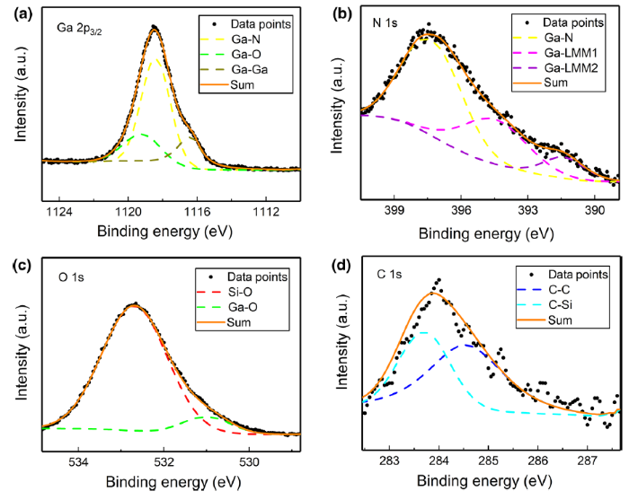
The GaN-graphene interface is crucial for the performance of high-power/high-frequency electronic devices. The etching rate for the sample was about 0.13 nm/s. Hence, the sample was etched for 600 s (78 nm) to get the XPS results measured at GaN/graphene interface. Ga 2p3/2, N 1s, C 1s and O 1s high-resolution XPS scans from the interface are displayed in Fig. 1. Ga 2p3/2 scans were fitted using three components. The main peak of the Ga 2p3/2 spectra is at 1118.4 eV corresponding to Ga-N bond. And this value is in accordance with the value (1118.5 eV) from previous observation. Ga-Ga and Ga-O bonding states are observed at 1116.34 eV and 1119.17 eV in Ga 2p3/2 HR-XPS spectra of the sample, respectively [27, 28, 29, 30]. The N 1s spectrum was also fitted using three subpeaks. The strongest one indicates predominant Ga-N bonding with peak position at 397.27 eV for 78-nm-thick GaN. The two small subpeaks correspond to Ga-LMM auger peak [26]. From Fig. 1c, two peaks are found from O 1s high-resolution XPS scans. One peak at 532.68 eV corresponds to Si-O bond which arises from the SiO2 substrate. The other is at 530.96 eV. According to research published before, the O 1s peak around 529-530 eV is attributed to lattice oxygen. The peak around 530.7-531.6 eV is ascribed to non-ideal chemical ratio of oxygen [31]. Hence, the high-resolution XPS scans of Ga 2p3/2 and O 1s indicate the existence of Ga-O-N compounds. However, the peak intensity reveals that only a small amount of Ga-O-N compounds are existed. In Fig. 1d, the binding energy (BE) value of the strong peak of C 1 s spetra is 284.54 eV which results from multilayer graphene [32, 33]. The weak peak (BE = 283.7 eV) represents the Si-C bond, which may be produced by ion etching [33]. These results show that the GaN/graphene heterostructure was formed with a low impurity concentration. The results also predict the existence of sharp interface between GaN and graphene which will be confirmed by XRR and TEM.
Fig. 1 High-resolution XPS scans of Ga 2p3/2, N 1s, O 1s and C 1s obtained from GaN-graphene interface
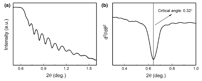
XRR data of the sample are shown in Fig. 2a. The clear oscillating curve in Fig. 2a corroborates that the interface between the GaN film and graphene is sharp. The curve in Fig. 2a depicts a rapid decline when the 2θ value ranges from 0.4° to 0.7°. This is the critical angle. Its value is primarily determined by the film density. The second derivative of the XRR data is presented in Fig. 2b for the purpose of better determining the critical angle value. The value is 0.32° which is in line with the result (0.32°) given by Motamedi et al. [34]. Then, the XRR data were fitted by the software using a four-layer model, i.e., GaN/graphene/SiO2/Si was used to obtain the GaN thin films density, thickness and roughness. The density, thickness and roughness given through the method are 5.44 g/cm3, 78 nm and 2.27 nm, respectively. These results indicate that the GaN-graphene interface is sharp and the GaN film has a good quality.
Fig. 2 a XRR measurement of GaN deposited on MLG templates and b critical angle extraction
Deminskyi et al. [35] demonstrated that the damage on MLG surface was caused by N2/H2 plasma. The Raman spectra were taken at room temperature using 532-nm laser to make sure that the graphene template is still in good condition after deposition. Figure 3a shows the Raman spectra of the sample before and after the GaN deposition. The graphene G peak is clearly visible after the deposition, and 2D peak of graphene can be also found. This indicates that the good properties of graphene are maintained [36]. Raman spectra are also used to study the crystallization and strain of the GaN. To focus on the GaN layer, 325-nm He-Cd laser was used. Peak of Si was used to compare with 520.7 cm-1 for calibration. Clear A1 LO mode for the GaN sample is found from Fig. 3b. The full width at half maximum (FWHM) of the peak predicts that the GaN film is polycrystalline. The peak position given by the spectrum is 723 cm-1. The phonon frequency (A1 LO) of as-deposited GaN film has a red shift by 11 cm-1 compared to strain-free GaN (734 cm-1) [37]. The red shift reveals the presence of residual tensile stress. The value of the tensile stress will be given by XRD.
Fig. 3 Raman spectra of the sample of a graphene before (blue line) and after (black line) deposition and b the as-deposited GaN
GIXRD was used to investigate the crystalline nature of the as-deposited GaN. Diffraction peaks presented in Fig. 4 prove the as-deposited GaN is polycrystalline which supports the Raman result shown before. The diffraction peaks at 32.4°, 34.5°, 36.7°, 57.6°, 69° and 70.3° are corresponding to the (100), (002), (101), (110), (112) and (201) planes of hexagonal GaN, respectively (PDF card No. 00-050-0792) [38]. And the diffraction peaks at 51.9° and 56.1° are caused by SiO2/Si templates. The cubic phase of the GaN was not detected. Therefore, the GaN film was a single-phase wurtzite (hexagonal) crystal structure. Crystallite size value of the sample was calculated from the (100), (002), (101), (110), (112) and (201) reflections using the Williamson-Hall plot. The value was found to be 15.8 ± 1 nm which is confirmed via TEM (Fig. 5c). The (002) reflection was also used to determine the lattice parameter c. Using the Bragg’s law, the value of interplanar spacing was evaluated from the peak position. Then, the following equation is given to determine lattice parameter c:
$\frac{1}{{d^{2} }} = \frac{4}{3}\left( {\frac{{h^{2} + hk + k^{2} }}{{a^{2} }}} \right) + \frac{{l^{2} }}{{c^{2} }},$ (1)
where d is interplanar spacing value, and h, k, l are the indices of crystal face.
Fig. 4 GIXRD pattern of the as-deposited GaN
Fig. 5 a, b Low-magnification cross-sectional TEM image of the as-deposited sample, c TEM image of GaN, d selected area electron diffraction (SAED) pattern of GaN
The c-axis lattice parameter given by the method is 5.1938 Å. And the c-axis lattice parameter of bulk GaN is 5.1855 Å. The strain of the sample obtained by comparing these two values is 0.16%. The value is consistent with the result (0.2-0.4%) reported in Ref. [17]. It indicates the presence of a minor tensile stress in the as-deposited film.
The film thickness of the sample measured using TEM is 78 nm. Figure 5a, b shows that the GaN thin films are pinhole-free and uniform. Besides, the GaN/graphene interface is sharp. In Fig. 5c, it can be seen that the area II of the GaN is completely crystallized. Besides, each individual crystallite has a cone-like top which affects the surface morphologies of the sample. According to the chemical analysis shown before, a small amount of Ga-O-N compounds are existed near the GaN-graphene interface. Therefore, the area I of the GaN is composed of GaN crystallites and Ga-O-N amorphous matrix composites. Ozgit et al. [39] reported similar results. The SAED pattern of the sample is shown in Fig. 5d. The result reveals the phase of GaN was hexagonal which is in line with the XRD result.
To further investigate the nucleation behavior of GaN deposited on graphene, the high-resolution transmission electron microscope (HRTEM) images are given in Fig. 6a, b and the GaN-graphene interface and graphene-SiO2 interface are clearly identified. Graphene displayed in Fig. 6a is continuous, while the graphene shown in Fig. 6b is incomplete. The inset image is FFT of the selected square area. Comparing the two inset images, it is found that the GaN deposited on incomplete graphene has a higher crystal quality. The explanation for this phenomenon is given as follows. Since the deposition of GaN on graphene is defect-selective, the GaN is easy to deposit on the graphene with defects which can provide surface groups. During each ALD cycle, nucleation events randomly occur over the surface of the amorphous regions of the GaN [40]. Therefore, GaN thin films deposited on the graphene with defects are easier to crystallize.
Fig. 6 HRTEM images of the GaN/graphene interface and (inset) FFT of the selected square areas
The XRR and TEM results show that the GaN grown on multilayer graphene has sharp interface and smooth surface. This is crucial for the application in the high-frequency and optical devices area.
The surface profile of the sample was directly studied using AFM. As shown in Fig. 7, the root mean square (RMS) value of surface roughness measured from 5 μm × 5 μm scan area of the as-deposited GaN is 2.52 nm. As mentioned before, individual crystallite with a cone-like top can affect the surface morphology. Thus, island-like granules and carinate surface can also be found in Fig. 7. Those are the upper surfaces of the GaN crystallites.
Fig. 7 Surface morphology of GaN thin film
Figure 8 shows the room temperature photoluminescence spectrum (PL) of the as-deposited sample. The optical band gap value of the sample is 3.62 eV, which is higher compared to the bulk GaN (~ 3.4 eV). The same value reported by Kizir et al. is 3.61 eV. This may be caused by the smaller grain/crystallite structure proved by the TEM results [26]. A blue luminescence band and a red luminescence band were also found from the spectrum. The center of the blue luminescence band and the red luminescence band is at 451 nm (2.75 eV) and 640 nm (1.94 eV), respectively. Blue luminescence is believed to be due to deep donor-shallow acceptor pair recombination, and red luminescence is believed to be due to donor to valence band transition [41].
Fig. 8 Room temperature photoluminescence spectrum of the sample
In summary, GaN thin film has been directly grown on multilayer graphene at a low temperature of 350 °C by PEALD and the graphene template is in good condition after the deposition. The GaN thin films were deposited with low impurity concentrations. It was proved that the sample is polycrystalline hexagonal with a minor tensile stress. The results of TEM, XRR and AFM indicate the GaN thin films are uniform and pinhole-free. And the GaN-graphene interface is sharp. Furthermore, it is found that the GaN deposited on defected graphene has a higher crystal quality because graphene with defects can provide surface groups which are important for the initiation of ALD growth. The results help to understand the deposition of GaN on graphene via PEALD at a temperature. This study provides a good method to deposit nanoscale GaN thin film on graphene at a low temperature which lays the foundation for improving the performance of GaN-based optical and high-power devices.
This work was supported financially by the National Natural Science Foundation of China (No. 110751402347), the Beijing Natural Science Foundation (Nos. 4173077 and 2184112), the Fundamental Research Funds for the Central Universities, China (Nos. FRF-BR-16-018A, FRF-TP-17-022A1, FRF-TP-17-069A1 and 06400071), the China Postdoctoral Science Foundation (No. 2018M631333) and the Youth Innovation Promotion Association of Chinese Academy of Sciences (No. 2015387).
The authors have declared that no competing interests exist.

 WeChat
/
| 〈 |
|
〉 |


