Search for articles:
Yue-Ling Guo , Bin Kong
Corresponding authors:
Received: 2017-07-22
Revised: 2017-08-28
Online: 2018-05-20
Copyright: 2018 Editorial board of Acta Metallurgica Sinica(English Letters) Copyright reserved, Editorial board of Acta Metallurgica Sinica(English Letters)
More
Abstract
Spherical Nb-20Si-24Ti-2Cr-2Al pre-alloyed powders were processed by selective laser melting (SLM) on Ti6Al4V substrates with different energy densities. A series of single tracks and single layers were produced using different processing parameters, including powder size, laser power, scanning speed and hatch distance. Results showed that the pre-alloyed powders ranging from 45 to 75 μm were more applicable to SLM with less balling tendency, in comparison with those between 75 and 180 μm. The increase in linear energy density (LED) resulted in the decrease in contact angle and the increase in the width of single track as well as its penetration depth into the substrate. Smaller hatch distance leaded to a larger remelted part of the former track and a higher volumetric laser energy density. With a thickness of 75.6 μm, an interfacial intermediate layer, enriched in Ti and depleted in Nb, Si, Cr and Al, was formed between the SLM part and the Ti6Al4V substrate. The mechanisms of the elimination of balling phenomenon by employing a higher LED and the interfacial bonding characteristics between Nb-Si-based alloys via SLM and the Ti6Al4V substrate were discussed.
Keywords:
Nb-Si-based ultrahigh temperature alloys have been widely investigated due to their potential application in the hottest sections of advanced turbine engines [1, 2]. Nb-Si-based alloys have been fabricated by a series of processes, e.g., arc melting [3], investment casting [4], directional solidification [5] and powder metallurgy [6]. Obtaining a proper dovetail geometry of the airfoil is normally a complex endeavor, requiring numerous time-consuming, post-machining operation [4]. More state-of-the-art techniques are in dire need of development to fabricate turbine blades from Nb-Si-based alloys with required performance.
Selective laser melting (SLM) is a kind of method of laser-based additive manufacturing technology, through which alloys can be rapidly manufactured into near net-shape components from pre-alloyed powders [7, 8]. Apart from simplifying the manufacturing procedures, SLM can be used to design materials and produce materials with improved performance [9, 10, 11]. Attar et al. [9] prepared a novel type of in situ Ti-TiB composites by SLM, which showed superior mechanical properties than SLM-produced pure Ti, owing to strengthening and hardening effects of the TiB particles and grain refinement of the α-Ti matrix. Gu et al. [10] found that the TiC/AlSi10Mg nanocomposites with a novel reinforcement architecture fabricated by SLM exhibited an enhanced mechanical property, compared with the unreinforced AlSi10Mg parts. Zhou et al. [11] presented that as-SLMed titanium alloys exhibited higher oxidation resistance and hardness than as-casted one. However, the SLM processing of Nb-Si-based alloys using sphere-shaped powders has scarcely been reported.
SLM is a complex physicochemical process, featured by the laser-powder-atmosphere interaction. Powder morphology, laser energy density, processing strategy and atmosphere tend to play very important roles in the printing process of SLM. Sphere-shaped powders are typically used for laser-based additive manufacturing, due to their excellent flowability and positive effects on the mechanical properties [12, 13]. The Ti-TiB composites built from 2-h milled powders, with nearly spherical shapes, typically exhibited higher relative density, greater compressive strength and strain than those produced from 4-h milled powders [13]. It is worth noting that the SLM process has a nonlinear response when the parameters are modified [14]. The defects including pores and cracks are prone to be caused by improper processing parameters of SLM, which are detrimental to mechanical properties for different types of materials, e.g., of Ti-6Al-4V components [15], β-type titanium porous structures [16], biomedical Ti-24Nb-4Zr-8Sn scaffolds [17] and Al86Ni6Y4.5Co2La1.5 metallic glass [18]. It is noteworthy that Harrison et al. [19] presented that the resistance to cracking of an alloy could be improved by increasing the concentration of substitutional solid solution strengthening atoms within the lattice.
It is known that SLM is a track-by-track and layer-by-layer process, and the formation of sound tracks well bonded to the substrate is required to build parts with high quality. In this work, a series of single tracks and single layers were directly formed on a Ti6Al4V substrate with different energy densities, and their forming characteristics as well as the molten pools were emphasized. The interfacial character of chemical distribution was also investigated.
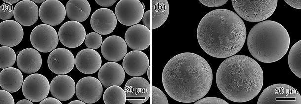
With a nominal composition of Nb-20Si-24Ti-2Cr-2Al (at.%), two kinds of Nb-Si-based alloy pre-alloyed powders (P1 and P2) were prepared by PREP in Ar atmosphere, aiming to study the effect of powder size on the interfacial bonding characteristics between single tracks and the Ti6Al4V substrate. The diameters of P1 powders ranged from 45 to 75 μm and the diameters of P2 powders were from 80 to 200 μm. The spherically shaped P1 and P2 powders are displayed in Fig. 1. The machine for SLM experiments included a fiber laser with maximum power of 500 W, an automatic powder delivery system, a building platform and a computer system for operation control. Single tracks and single layers with different processing parameters were fabricated on ground Ti6Al4V substrates, using P1 and P2 powders as the starting materials, respectively. Before laser scanning, a single powder layer was spread on the Ti6Al4V substrate. The layer thickness was typically larger than the powder size. Thus, the separately deposited powder layers of P1 and P2 were 80 and 200 μm in thickness. The scanning lines were 12 mm in length. In case of any oxidation, the building chamber was vacuumed and then filled with Ar atmosphere prior to SLM processing. The residual oxygen level was kept below 0.1 wt% in the building chamber. A cubic part was further printed with optimized processing parameters to study the interfacial characteristics between the Ti6Al4V substrate and Nb-Si-based alloy via SLM. The processing parameters were: laser power 340 W, scanning speed 500 mm/s, hatching distance 0.10 mm and layer thickness 0.08 mm.
Fig. 1 Surface morphologies of Nb-Si pre-alloyed powders: a P1; b P2
Surface morphologies were examined using a scanning electron microscope (SEM, Quanta 200F). Microstructure analysis was performed using an electron probe microanalyzer (EPMA, JXA-8230) and SEM with backscattered electron imaging (BEI). For analyzing the cross-sectional microstructure, the samples were mounted, ground and polished according to standard procedures.
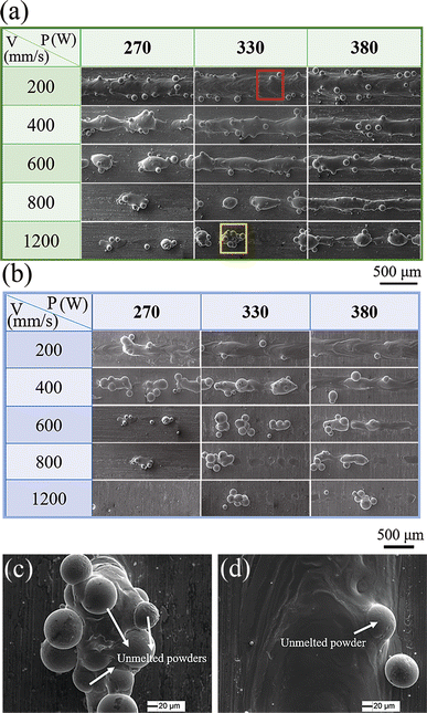
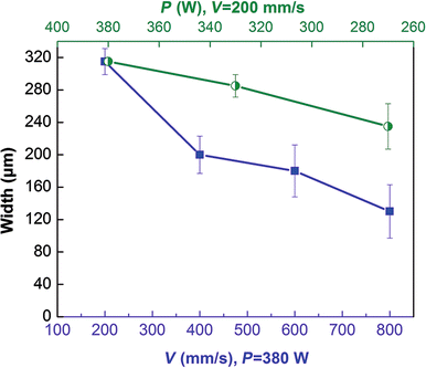
Figure 2 shows the typical surface morphologies of the first-layer single tracks formed from P1 and P2 powders at different scanning speeds and laser powers. Both stable and unstable single tracks were observed: The former ones are featured by stable molten pools and continuous tracks; the latter ones are presented by the formation of drops and discontinuous tracks. These drops, i.e., fragmentations of the single tracks, refer to the balling phenomenon, an unfavorable drawback of SLM [20, 21]. Unmelted Nb-Si-based pre-alloyed powders are bonded to both the continuous and the discontinuous tracks, as shown in Fig. 2c, d, probably caused by the high viscosity of Nb-Si melt at high temperature. It suggests that the stability of a single track depends largely on the SLM processing parameters, e.g., laser power, scanning speed and physical property of the starting powders. By either decreasing the scanning speed or increasing the laser power, the balling phenomenon could be eliminated and continuous single tracks are thus yielded. As displayed in Fig. 2a, there are eight continuous single tracks formed from P1 powders with the processing parameters given in this work. In contrast, only one continuous single track is formed from P2 powders using the same parameters as that for P1 powders (Fig. 2b). It demonstrates that P1 powders ranging from 45 to 75 μm are applicable to SLM, while P2 powders with larger diameters are unlikely to be well processed by SLM. Namely, for Nb-Si-based alloys, the increase in the layer thickness can increase the balling tendency, which is in accordance with the results presented by Wang et al. [22]. Figure 3 shows the width distributions of the single tracks formed from P1 powders and the average width of the single track is also closely related to the processing parameters of SLM. With a consistent scanning speed of 200 mm/s, the width of the single track increases with the increase in laser power. Meanwhile, with a fixed laser power of 380 W, the width decreases with the increase in scanning speed. The reason behind this phenomenon is that the increase in laser power and the decrease in scanning speed typically produce a larger volume of liquid Nb-Si melt, leading to the formation of wider track resultantly.
Fig. 2 Surface morphologies of single tracks formed from P1 a and P2 b powders; c is the magnified image of the yellow rectangle in a, d is the magnified image of the red rectangle in a
Fig. 3 Width distributions of single tracks formed from P1 powders with different processing parameters (the error bars refer to standard deviation)
The typical sectional microstructure of the single tracks formed from P1 powders is presented in Fig. 4. The single track was processed with a laser powder of 380 W and a scanning speed of 400 mm/s. Apparently, the single track is bonded to the Ti6Al4V substrate, featured by a dagger-like penetration into the substrate, which is typically observed in the microstructures of alloys processed by SLM [16, 23]. The sub-circular morphology may result from the Gaussian distribution of the laser beam and the competition between heat transfers through convection and conduction in the melt pool [24]. The penetration depth in the middle of each single track is larger, probably because the energy concentration is higher in the center of laser beam spot. Across the melt pool, a severe chemical segregation is observed. The darker parts tend to be rich in Ti, and the lighter parts are normally rich in Nb. Figure 4b shows the distributions of Nb, Si and Ti along line OA drawn in Fig. 4a. The fluctuations in intensity of alloying elements provide additional evidences on the chemical segregation in the melt pool.
Fig. 4 a Cross-section morphology of single track formed from P1 powders (P = 380 W, V = 400 mm/s); b distributions of Nb, Si and Ti elements along line OA obtained using EPMA
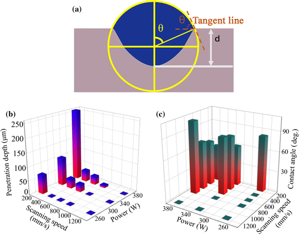
A schematic plot of contact angle (θ) and penetration depth (d) is illustrated in Fig. 5a, and the analyzing results of the eight continuous single tracks formed from P1 powders are displayed in Fig. 5b, c. With different processing parameters, the contact angle and the penetration depth of the single tracks vary significantly. The contact angle, indicating the wettability between the Nb-Si-based alloy melt and the Ti6Al4V alloy, increases with the increase in scanning speed and the decrease in laser power. Inversely, the penetration depth into substrate decreases with the increase in scanning speed and the decrease in laser power.
Fig. 5 Schematic plot of contact angle (θ) and penetration depth (d) of single tracks a; penetration depth b and contact angle c on cross-sections of single tracks formed from P1 powders
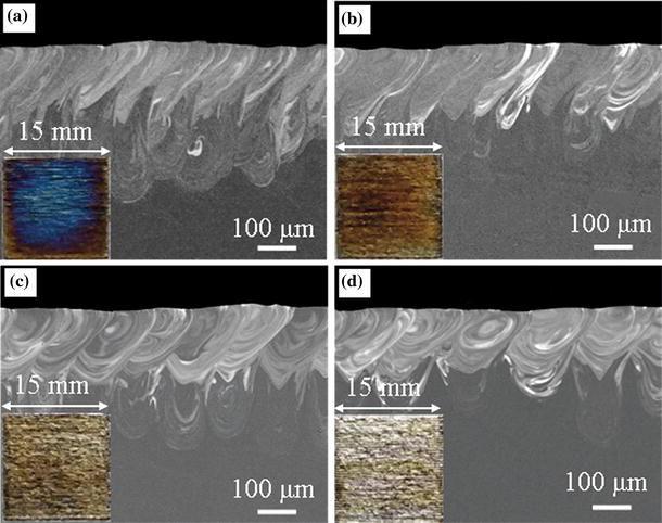
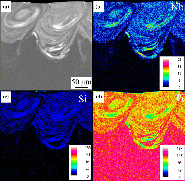
A single SLM layer is formed through the superposition of the single tracks, and thus it would be necessary to investigate the single layer formation with different hatch distances (shift between two neighboring tracks, H). Figure 6 shows the macroscopic surface morphologies and cross-sections of the single layers with four different hatch distances (50, 80, 120 and 150 μm). The laser power is 380 W, and the scanning speed is 200 mm/s. It is obvious that the surface color grows from yellow to blue with the decrease in hatch distance, which should be closely related to the oxidation of titanium in the melt pool, when suffering from high laser energy input during the SLM process [25]. Moreover, a lower hatch distance indicates a larger remelted part of the previously deposited track. It is necessary to remelt parts of the former tracks to produce a metallurgical bond between two adjacent tracks. But an excess of the remelted part may greatly alter the microstructure and the chemical element distribution of the former track, and an overlarge hatch distance may fail to remelt parts of the former tracks to produce a metallurgical bond. Chemical distributions of main elements of Nb, Ti and Si are shown in Fig. 7. Evidently, a heterogeneous distribution of these main elements is observed. The melt pool is featured by the existence of swirl-like patterns, which is probably the result of convection-enhanced mass transport [18, 26, 27].
Fig. 6 Cross-section morphologies of single layers formed from P1 with different hatch distances (H): a H = 50 μm; b H = 80 μm; c H = 120 μm; d H = 150 μm. The laser power is 380 W, and the scanning speed is 200 mm/s. The insets in the bottom show the macroscopic surface morphologies of the single layers processed with respective hatch distance
Fig. 7 Chemical maps of cross-sections of single layers formed from P1 with different hatch distances in sub-circular interfacial region: a BEI; b Nb; c Si; d Ti
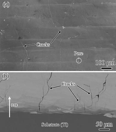
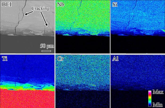
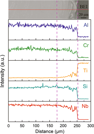
As shown in Fig. 8a, a continuous and sound intertrack bonding is presented on the top surface of a SLM-processed part with 4 mm in height. The balling phenomenon has been suppressed, mainly due to the optimization of processing parameters. Cracks and pores are observed on the top surface. As stated in our previous work [28], cracking normally takes place during the SLM processing of brittle Nb-Si-based alloys. Figure 8b shows the microstructure of the interface between the Ti6Al4V substrate and Nb-Si-based alloy via SLM. Apart from the top surface, some cracks are also observed inside the Nb-Si-based alloy built by SLM. Figures 9 and 10 show the distributions of Nb, Si, Ti, Cr and Al on the interfacial area, in order to study the chemical composition of Nb-Si-based alloys processed by SLM on Ti6Al4V substrate. Obviously, an intermediate layer is noted, which is enriched in Ti and depleted in Nb, Si, Cr and Al. The fluctuation in the intensity indicates a heterogeneous distribution of each element, i.e., the occurrence of chemical segregation (Fig. 10). It could thus be inferred that during SLM, accompanying with the melting of P1 powders, the Ti6Al4V substrate is partly melted and involved into Nb-Si-based alloy. Consequently, the intermediate layer is generated, with a higher Ti content compared with that in the Nb-Si-based alloy. It suggests that during the SLM processing of Nb-Si-based alloy, the firstly printed several layers are contaminated by Ti from the substrate. As shown in Fig. 10, the intermediate layer is about 75.6 μm in thickness, which is slightly thinner than the layer thickness of SLM processing (80 μm). It is safe to conclude that at least two layers are contaminated by Ti from the substrate, as the shrinkage of Nb-Si-based pre-alloyed powders is known to occur after melting and solidification during SLM [22].
Fig. 8 Top surface a and sectional microstructure b of cubic part built by optimized processing parameters
Fig. 9 Chemical maps of interface between Ti6Al4V substrate and Nb-Si-based alloy via SLM: a BEI; b Nb; c Si; d Ti; e Cr; f Al
Fig. 10 Distributions of Nb, Si, Ti, Cr and Al across interface between Ti6Al4V substrate and Nb-Si-based alloy via SLM
As shown in Fig. 2, the balling phenomenon could be eliminated by either decreasing the scanning speed or increasing the laser power, both of which intrinsically result in an increase in the linear energy density (LED, laser energy per unit length). LED is identified by as follows:
${\text{LED}} = \frac{P}{V},$ (1)
where Ρ is the laser power and V is the scanning speed. The energy of laser beam is absorbed by the first layer of powders, leading to the melting of powders. The volume of the liquid phase mainly hinges on LED during single linear laser scanning, and a smaller volume of liquid phase typically results from a lower LED. Meanwhile, the increase in the viscosity of the liquid-solid mixture reduces the flow ability of the liquid phase and decreases the overall rheological performance of the liquid in conjunction with powders [20, 29]. Consequently, the liquid Nb-Si alloy melt tends to aggregate into a coarsened sphere, with some unmelted and semi-melted powders “welded” on the surface (Fig. 2c). Molten cylinders break up to achieve an equilibrium state with a reduced surface energy, namely the emergence of balling phenomenon. Though some semi-melted powders are also “welded” on the stable single tracks, the enough volume and high flow ability of the liquid guarantee the formation of continuous tracks (Fig. 2d). If the length of the molten free circular cylinder formed from Nb-Si-based alloys is larger than its circumference (the limit of the Plateau-Rayleigh capillary instability), it tends to break up into several droplets, i.e., the balling phenomenon takes place [30].
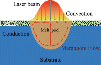
Figure 11 displays the schematic diagram of the SLM physical model. The laser beam with a Gaussian power distribution works as a heat source for SLM. A series of physical phenomena occur in an essential operation of SLM: absorption and scattering of laser radiation, heat transfer, powder melting, fluid flow within the molten pool and solidification [26, 27]. The interaction time between the laser beam and starting powders is typically the order of ~ 1 ms [24, 31]. In such an extremely short time scale, the heat flow distance is far less than the powder diameter. Resultantly, the skins of the Nb-Si-based alloy powders are heated up rapidly, followed by the transference of the absorbed energy to the surroundings through thermal diffusion [32]. The exposed powders tend to be fully melted, when heated up to exceed their melting point. The responsible reasons for the undesirable SLM formality of P2 are stated as follows. On the one side, larger powders provide a higher porosity and smaller surface area. Resultantly, less laser energy is absorbed and the powers are more difficult to be melted [31, 33]. The unmelted or semi-melted large powders involved in the liquid phase may reduce its flow ability and deteriorate its overall rheological performance [20, 29]. Accordingly, single tracks formed from P2 powders exhibit an aggravated balling phenomenon. Enough volume of liquid Nb-Si melt is necessary for the formation of a continuous and sound single tracks. This may be achieved with a higher laser power and a lower scanning speed, i.e., higher LED. On the other side, the powders with larger diameters normally form a thicker powder bed, as the thickness of powder bed should be larger than the diameter of powders. During laser scanning, only a part of laser energy is absorbed by the outmost powders and the residual laser energy penetrates through the pores containing gases and interacts with the underlying particles. The intensity of laser energy decreases with its penetration into the powder bed. Thus, bottom powers absorb less laser energy. Similarly, other investigations have reported that the thickness of the powder bed affects the continuity of single tracks and the relative density of the component fabricated by SLM [14, 26, 34].
Fig. 11 Schematic diagram of SLM physical model
The process of single SLM-track fomentation is featured by the interaction of two dissimilar metals with different thermophysical properties, namely the interaction of Nb-Si alloy powders and Ti6Al4V substrate. Metallurgical nature of the interaction area tends to largely determine the mechanical performance of a component processed by SLM [24, 35]. The increase in LED is typically associated with higher laser power and lower scanning speed, and this explains the larger values of both the width and the penetration depth of the single tracks, which is in accordance with the results reported by Liu et al. [16]. It is worth noting that the penetration depth is larger than the thickness of the first powder layer (80 μm) with the maximum power (380 W) at minimum scanning speed (200 mm/s), as shown in Fig. 5b. The electron beam can be reflected by the inner surface of the deep melt pool, resulting in the concentration of power and resultant higher temperature at the bottom [16]. Therefore, the laser beam, with a larger LED value, tends to penetrate deeply into the substrate, and an overlarge penetration depth forms.
High laser beam energy induces an intensive heat transfer. The temperature gradient, resulting from the heat transfer, generates coupled heat and mass transfer process. A melt pool will be generated with the formation of Marangoni convection, the thermocapillary flow of a fluid from one region with a low surface tension to other region with a high surface tension. During the SLM process, the microstructure of a component built by SLM tends to largely depend on the convection in the melt pool. Dai and Gu [36] presented that the emergence of swirl-like pattern suggests that thermocapillary convection plays a dominant role in the heat transfer process, rather than conduction. The interfacial intermediate layer formed on the substrate is believed to be caused by the convection-enhanced mass transport.
Considering the thickness of the power bed (S) and hatch distance, the volumetric laser energy densities (VED) are defined by the following equation, instead of LED, to assess the laser energy input to the powder bed:
${\text{VED}} = \frac{P}{VHS}.$ (2)
It is observed that VED is inversely proportional to the hatch distance. The powder bed thus absorbs more laser energy when decreasing the hatch distance. The reduction of VED is responsible for the change of the color of single layer from yellow to blue with the decrease in hatch distance [25]. Namely, an excess of laser energy input will result in the oxidation of certain elements with higher oxygen affinity, e.g., Ti.
Based on the results mentioned above, the powder size, laser power, scanning speed and the hatch distance all play a key role in the SLM processing of Nb-Si-based alloy. The mechanisms have been analyzed in this work. This is very helpful to build a component of Nb-Si alloy with desired mechanical performance.
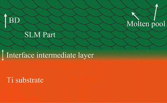
A cubic part has been successfully built via SLM, featured by a continuous and sound intertrack bonding (Fig. 8). An identical top surface was reported previously for the Nb-Si-based alloys using jet milled powders with irregular shapes [28]. This will benefit the formation of a dense layer and result in a dense SLM component. Half-cylindrical molten pools were displayed on the vertical section, i.e., paralleling to the building direction [28]. Furthermore, Fig. 12 shows the typical microstructure of Nb-Si-based alloy processed by SLM on a Ti6Al4V substrate. Each track is bonded to the neighboring track in three-dimensional space. Molten pools were observed in the sectional microstructure. The SLM part built from Nb-Si-based alloy is well bonded to the Ti6Al4V substrate. An interfacial intermediate layer, enriched in Ti and depleted in Nb, Si, Cr and Al, is formed between the SLM part and the Ti6Al4V substrate. The interfacial intermediate layer is thinner than the thickness of the powder bed for SLM. It suggests the composition of the bulk Nb-Si-based alloy part via SLM will not be altered by the Ti6Al4V substrate, by excluding the first several layers of the bulk part.
Fig. 12 Microstructural illustration of Nb-Si-based alloy processed by SLM on a Ti6Al4V substrate
1. The Nb-20Si-24Ti-2Cr-2Al pre-alloyed powders ranging from 45 to 75 μm were more applicable to SLM, compared with those ranging from 75 to 180 μm. With the processing parameters employed in this work, the balling phenomenon was able to be eliminated by employing a higher LED, i.e., decreasing the scanning speed or increasing the laser power.
2. With the increase in LED during SLM, the width of the single track and its penetration depth into the Ti6Al4V substrate increased, while the contact angle decreased. The melt pool formed by the melting of powders was featured by a heterogeneous distribution of alloying elements in swirl-like patterns.
3. The decrease in the hatch distance leaded to a larger remelted part of the former track and a higher VED. An excess of laser energy input typically caused the oxidation of Ti in the melt pool.
4. An interfacial intermediate layer, enriched in Ti and depleted in Nb, Si, Cr and Al, was formed between the SLM part and the Ti6Al4V substrate. Its thickness was 75.6 μm, which was slightly thinner than the layer thickness of SLM processing (80 μm).
Acknowledgements This work was supported financially by the National Natural Science Foundation of China (Nos. 51471013 and 51571004).
The authors have declared that no competing interests exist.

 WeChat
/
| 〈 |
|
〉 |
