Search for articles:
S. Shanmugan , D. Mutharasu
Corresponding authors:
Received: 2016-09-16
Online: 2018-01-20
Copyright: 2018 Editorial board of Acta Metallurgica Sinica(English Letters) Copyright reserved, Editorial board of Acta Metallurgica Sinica(English Letters)
More
Abstract
Boron-doped aluminum nitride (B-AlN) thin films were synthesized on Al substrates by using chemical vapor deposition method by changing the synthesis parameters and were used as thermal interface material for high power light emitting diode (LED). The B-AlN thin film-coated Al substrate was used as heat sink and studied the performance of high power LED at various driving currents. The recorded transient cooling curve was evaluated to study the rise in junction temperature (Tj), total thermal resistance (Rth-tot) and the substrate thermal resistance (Rth-sub) of the given LED. From the results, the B-AlN thin film (prepared at process 4) interfaced LED showed low Rth-tot and Tjvalue for all driving currents and observed high difference in Rth-tot (ΔRth-tot = 2.2 K/W) at 700 mA when compared with the Rth-tot of LED attached on bare Al substrates (LED/Al). The Tj of LED was reduced considerably and observed 4.7 °C as ΔTj for the film prepared using process 4 condition when compared with LED/Al boundary condition at 700 mA. The optical performance of LED was also tested for all boundary conditions and showed improved lux values for the given LED at 700 mA where B-AlN thin film was synthesized using optimized flow of Al, B and N sources with minimized B and N content. The other optical parameters such as color correlated temperature and color rendering index were also measured and observed low difference for all boundary conditions. The observed results are suggested to use B-AlN thin film as efficient solid thin film thermal interface materials in high power LED.
Keywords:
In microelectronic technology, heat management has become one of the important concerns in relation to miniaturization of electronic packaging, especially in advancement and evolution of light emitting diodes (LEDs). The efficiency of LEDs strongly depends on the heat dissipation from PN junction to ambient [1]. It was proved that lifetime of a LED decays exponentially as the device temperature increases [2]. In order to extend the life of the LEDs, proper heat path must be established and addressed.
In the design of LED system, heat sink is one of the key components in cooling solution for LEDs. However, the contact surface area between heat sink and LED package has significant effect on the heat propagation from package to ambient [3]. This issue is usually compensated by thermal interface material (TIM) [4]. Thermal grease has been a common TIM with increasing total contact area between LED package and heat sink [5]. Several works had been reported on thin film-based thermal electric cooler for LED system [6, 7].
Group III nitrides are highly recommended as heat dissipation coating due to its significance in thermal conductivity [8], and the aluminum nitride (AlN) is one of the nitride groups which is attractive in this application. Theoretically, the thermal conductivity of AlN is reported to be about 280 W m-1 K-1 [9]; however, the typical value of polycrystalline AlN thin film was reported in the range of 9.9-26.7 W m-1 K-1 [10]. Thin film thermal conductivity is very much depending on the deposition method and process conditions [11]. There are only a few studies on the combination of group III elements such as boron and aluminum in nitride thin film for thermal application, and they reported that the thermal conductivity can be improved by boron doping which shrinks the lattice of AlN [12]. Our research group has already used AlN thin film as TIM and achieved good performance on reducing total thermal resistance (Rth-tot) and junction temperature (Tj) of the LED with respect to driving currents [13]. In addition, we have also used carbon-doped AlN thin film as interface material and succeeded on improving the performance of the given LED [14]. In our another study, the AlN and BN thin film was used as TIM and tested the LED performance, and we noticed an improved light output and reduced thermal resistance (Rth) and Tj for the tested LED [15, 16].
In this work, B-AlN thin film was synthesized by CVD method using various synthesis parameters and was used as thermal interface materials. Al (99.5%) was used as substrate and considered for heat sink. In order to avoid the substrate melting and reduce the processing temperature, the operating condition of nitrogen source should be <650 °C (melting point of Al is 660 °C). Moreover, tert-buthylamine (ButNH2) (346 kJ/mol) was chosen as nitrogen source precursor since it has lower dissociation energy compared to NH3 (449 kJ/mol) [17, 18], and it was also proved to be a more effective nitrogen source producing good conductive nitride thin film when compared to NH3. In addition to ButNH2, trimethylaluminum (Me3Al) [19] and tri-tert-butylaluminum ( t Bu3Al) [20] were used at low deposition temperature (400-600 °C). The B-AlN-coated Al substrates were tested as heat sink with 3-W LED in the approach of enhancing the thermal and optical performances of given LED.
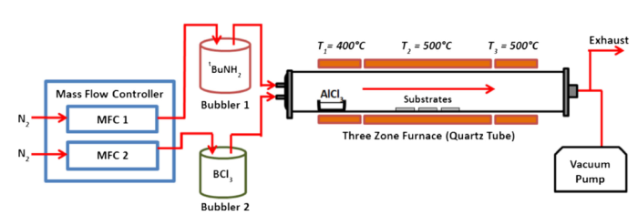
A hot-wall three-zone furnace attached with fused quartz tube was used for deposition of B-doped AlN thin film on Al substrates (25 mm × 25 mm × 3 mm). In order to change the elemental compositions of the thin film, various process conditions are designed by changing the flow rate of carrier gases and source materials. The detailed information of the process conditions is provided in Table 1. AlCl3powder (anhydrous sublimed ≥98%, Sigma-Aldrich), BCl3 solution (1 mol L-1 solution in hexane, Acros Organics) and tert-buthylamine solution (98%, Aldrich Chemistry) were used as Al, boron and nitrogen source for the synthesis of B-AlN coating, respectively. In this study, AlCl3 was chosen as Al source which circumvents the high reactivity of AlCl with the quartz (SiO2) reactor and is suitable for use as Al source like solid organic sources for metal organic vapor phase epitaxial (MOVPE) [21]. BCl3 is of great importance in chemical physics due to their nonpolar and highly plane symmetric (D3h) geometry. For this reason, BCl3 is extensively used in deposition and doping of boron [22].
Table 1 Deposition parameters of B-AlN thin film coating by CVD
| Process | Source material | Carrier gas (N2) flow rate (sccm) | Average film thickness (nm) |
|---|---|---|---|
| Process 1 | AlCl3 | 10 | 423 |
| tert-buthylamine | 25 | ||
| BCl3 | 25 | ||
| Process 2 | AlCl3 | 2.5 | 498 |
| tert-buthylamine | 15 | ||
| BCl3 | 15 | ||
| Process 3 | AlCl3 | 5 | 440 |
| tert-buthylamine | 25 | ||
| BCl3 | 25 | ||
| Process 4 | AlCl3 | 5 | 418 |
| tert-buthylamine | 10 | ||
| BCl3 | 10 |
AlCl3 powder (~8 g) was filled in a boat-type crucible and positioned in the left zone of the furnace (Fig. 1). Al substrates were positioned at the center zone of the furnace. Initially, the CVD tube was evacuated by rotary pump and filled with N2 gas to maintain the inert atmosphere inside the tube and also avoid the air or other oxide contamination. Two different temperatures based on the evaporation temperature of the source and desired deposition temperature were fixed at CVD tube zones for this synthesis. The left zone was fixed at 400 °C to complete evaporation of AlCl3 powder, and the center zone was fixed at 500 °C for deposition. In order to avoid the deposition of unwanted chemicals on the inside wall of CVD tube, right zone was maintained at 500 °C. Air bubbler was employed for this synthesis in order to deliver the precursor (tert-buthylamine) into the deposition zone where N2 gas was used as carrier gas and their flow rate was controlled by digital mass flow controller (MFC). The tert-buthylamine vapor mixed with AlCl3 vapor at left zone was flow through the center of the CVD tube where the Al substrates are positioned for deposition (Fig. 1). The coating process was conducted for 1 h under atmospheric pressure. BCl3 solution was bubbled with N2 carrier gas into the tube at 30 min of process time. For thickness measurement, Si samples were also kept inside the CVD tube as reference during the deposition time and used for field emission scanning electron microscopy (FESEM) cross-sectional analysis to measure the thickness. The FESEM was operated at 10 keV which was minimized the charging effect and allowing the surface to be viewed without a conductive coating. The thickness was measured directly at various points, and the average is presented in Table 1 for discussion.
Fig. 1 Schematic diagram of synthesis of B-AlN thin film using CVD method
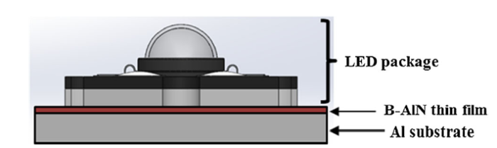
The thermal transient analysis was carried out for the given LED at three different driving currents (100, 350 and 700 mA) in a still-air chamber at room temperature where the B-AlN thin film was used as thermal interface material and tested their performance. B-AlN-coated Al substrates were used as heat sink by attaching the 3-W LED package with uniform pressure applied across the contacting surfaces. The schematic diagram of testing configuration is given in Fig. 2. Initially, the LED was forward biased for 900 s and the transient cooling curve of the LED package was captured for another 900 s. In addition, the transient cooling profile of the LED fixed on bare Al substrates was obtained and compared with the results of B-AlN thin film interfaced LED. All transient cooling curves were processed for structure functions analysis using Trister Master Software. Before we start the real measurement, the LED was thermally calibrated using dry thermostat with T3Ster as power supply. The product of K and the difference in temperature-sensing voltage (referred to as ΔVF) produces the device junction temperature rise.
Fig. 2 Schematic diagram of LED mounted on B-AlN-coated Al Substrate$ \Delta T_{\text{j}} = \, \Delta V_{\text{F}} K. $ (1)
During the calibration process, the LED was driven with lower operating current (1 mA) at room temperature 25 °C to prevent self-heating effect at the junction. The voltage drop across the junction was recorded once the LED reaches thermal equilibrium with the temperature of the thermostat. Later, the ambient temperature of the LED was varied from 25 to 75 °C at 5 °C step size and the voltage drop across the junction was recorded at each defined temperature. From the calibration process, the K-factor of the LED was determined from the graph of junction voltage (voltage drop) against ambient temperature as 2.866 × 10⁻³ V/°C.
The optical behavior of 3-W green LED package attached with B-AlN thin film-coated Al substrates was also analyzed. During the measurement, the device was burnt for 15 min at regulated input currents based on the electrical test method JEDEC JESD-51. The optical parameters of the given LED such as correlated color temperature (CCT), color rendering index (CRI) and brightness (Lux) were recorded for various driving currents (100, 350 and 700 mA) using optical meter (MK350 LED meter) made by UPRtek. The experiment was carried out in parallel with thermal measurement under regulated driving currents.
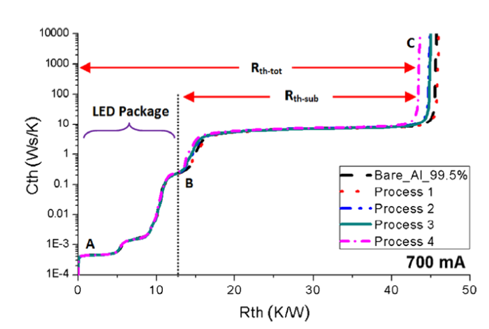
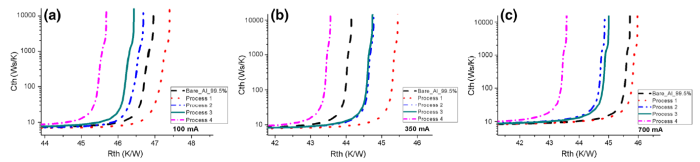
The thermal transient analysis was carried out for the given LED where B-AlN thin film was used as thermal interface material. The thermal transient curve was recorded at three different driving currents for each boundary condition and processed using T3Ster Master Software for cumulative structure function. Figure 3 shows the cumulative structure function measured at 700 mA. The total thermal resistance (Rth-tot) is measured across the entire curve to ambient (Points A-C), and the substrate thermal resistance (Rth-sub) is measured from the deviation point at interface between LED package and coated substrate to the ambient (Points B-C). In order to get the clear information on the performance, the Rth-tot of 100, 350 and 700 mA from cumulative structure function curves is magnified and shown in Fig. 4. Rth-tot and Rth-sub were also evaluated from the curves and are summarized in Table 2.
Fig. 3 Cumulative structure function of 3-W green LED fixed on B-AlN-coated Al substrates measured at 700 mA
Fig. 4 Zoomed version of cumulative structure function curve of 3-W green LED fixed on B-AlN-coated Al substrates measured at a100 mA, b 350 mA, c 700 mA
Table 2 Thermal resistance of 3-W green LED fixed on substrate prepared at various process conditions
| Driving currents (mA) | Bare Al | Process 1 | Process 2 | Process 3 | Process 4 |
|---|---|---|---|---|---|
| Junction to ambient total thermal resistance, Rth-tot (K/W) | |||||
| 100 | 46.96 | 47.40 | 46.70 | 46.43 | 45.67 |
| 350 | 44.18 | 45.43 | 44.78 | 44.71 | 43.52 |
| 700 | 45.74 | 45.94 | 44.85 | 44.98 | 43.54 |
| Board to ambient (substrate) thermal resistance, Rth-tot (K/W) | |||||
| 100 | 34.64 | 34.13 | 33.09 | 33.63 | 33.02 |
| 350 | 31.70 | 32.64 | 31.31 | 31.53 | 30.34 |
| 700 | 29.81 | 29.50 | 28.89 | 29.08 | 27.68 |
It clearly indicates that the Rth-tot of the LED changes for different driving currents and various process conditions of B-AlN thin film interface in the study. As we know, increase in driving current results in decrease in thermal resistance of the LED package [15]. Figure 4shows that the Rth-tot shows high value for the film prepared at process 1 condition and very low value could be noticed for the film prepared with process 4 condition. It is also understood that the higher driving currents improve the performance of the LED by reducing the Rth-tot considerably. As compared with bare conditions (bare Al) where no interface material was applied, the B-AlN thin film interfaced LED shows low Rth-tot value where the films were prepared with process 2, process 3 and process 4 conditions. On comparing bare Al boundary condition, difference in Rth-tot (ΔRth-tot) is high (2.2 K/W) for the LED measured at 700 mA where the B-AlN thin film interface was prepared using process 4 condition. It is suggested that the CVD synthesized B-AlN thin film is successful as thermal interface material to reduce the Rth-tot of the LED considerably. The reduction in Rth-tot is due to several effects: (1) The crystalline nature of the film will change into defect free conditions and expected to more heat transfer from the board to heat sink substrate and (2) the thermal conductivity of B-AlN thin film may increase as a result of temperature induced by rise in junction temperature of the device [23], and hence, low thermal resistance is possible at the interface.
On considering the synthesis parameters, the material compositions (Al, B and N) are expected to change with the flow rate of carrier gases. In our study, also, it is assumed that the material composition is changed with respect to the process conditions. As shown in Table 1, the aluminum content will be more with process 1 than with process 2 and it is believed that the B content (contributed by BCl3) increases in B-AlN thin film when it is prepared using process 1 and 2 conditions. The changes in material composition are reflected in the thermal resistance of the B-AlN thin film and hence change the thermal behavior of the LED when it is tested as thin film interface. As we expected more B content than Al content in B-AlN thin film using process 2 parameters, the low Rth-tot of LED is observed for process 2 at high driving current [24]. Further, when comparing the results of processes 1 and 4, the film processed under condition 1 is expected to have higher B content and also N content (contributed by tert-buthylamine) than the film processed under condition 4. It is addressed that the N content is expected to be high in thin films prepared at condition 1 and hence low thermal conductivity of the film [25, 26].
In processes 1 and 2, though B content is high, the N content is dominating and reduces the thermal properties of the prepared film. So the LED using the B-AlN thin film as interface prepared at conditions 1 and 2 shows high Rth-tot value. Moreover, the LED interfaced with B-AlN thin film prepared at condition 4 shows low Rth-tot and it is clearly seen that the optimized N, Al and B content is expected in B-AlN thin film samples prepared at condition 4, where the total gas flow rate is the lowest (25 sccm) as compared to all process conditions, and hence, the low Rth-tot is observed with this process condition. It is attributed to the effect of good conductivity behavior of B-AlN thin film as interface which is already proved in our previous work [27]. Overall, the thermal behavior of B-AlN thin film depends on the total N, Al and B content in terms of gas flow rate.
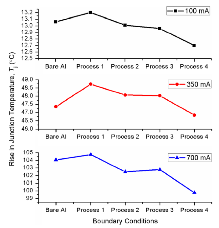
Consequently, the rise in junction temperature of the given LED was also evaluated from the cooling transient curve from which the cumulative structure function curves are evaluated. The measured Tj of the given LED for various boundary conditions are plotted in Fig. 5. As shown in Fig. 5, the Tj values change as the process condition changes. There is an increase in Tj for B-AlN thin film interfaced LED with 350 mA. As shown in Table 1, it is expected that the Al composition is high for the process 1 than all other process conditions and possible for current crowding [28, 29] which suppress the thermal conductivity across the film. So the film prepared at process 1 condition shows high Tj values in all driving currents.
Fig. 5 Variation of measured Tj of 3-W LED fixed on bare and B-AlN thin film-coated Al substrates prepared at various process parameters
As described above, the B-AlN thin film interfaced LED shows low Tj values than bare Al boundary condition and low value in Tj is recorded with B-AlN thin film interfaced LED where the thin film is prepared using process condition 4. As comparing bare Al boundary condition, the difference in Tj (ΔTj) is 4.74 °C for the LED using B-AlN thin film from process 4 and tested at 700 mA driving current which is high when compared with other boundary conditions as well as the driving currents. Moreover, no much difference in Tj is also noticed at <350 mA, which is because of insufficient energy to induce the molecular vibration (free electrons) within the material for thermal conduction [30].
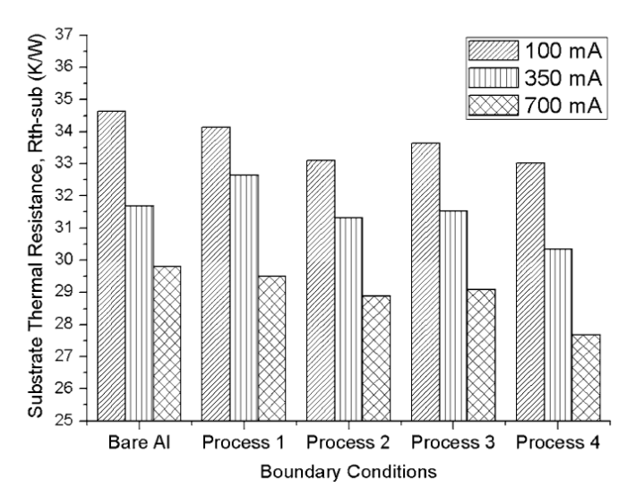
In addition to Tj and Rth-tot, the thermal behavior of interface material (B-AlN thin film) is discussed and the thermal resistance of the substrate (Rth-sub) is extracted from the cumulative structure function curve (Fig. 3) and plotted as shown in Fig. 6. It can be clearly indicating that Rth-sub reduces as the driving current increases. The Rth-sub is the lowest for the LED interfaced with film prepared at process 4 for all driving currents. Especially, the film prepared at process 4 condition shows low Rth-sub when the B-AlN thin film interfaced LED tested at 700 mA. As stated in the above discussion, the material (B-AlN) resistance changes with respect to the elemental content of the thin film (B, N and Al), and as a result of optimized material content, low value in Rth-sub is possible with the film prepared using condition 4. As shown in Table 1, the thickness of B-AlN thin film is also changing with process conditions and high and low thickness are noticed with thin films prepared at process 3 and 4 conditions, respectively. In the resistance analysis, according to Ref. [31], the film thickness is considered as bond line thickness and influences the heat flow and decides thermal resistance of the interface material in LED packaging. From the observed results, the Rth-sub and Tj decrease with decreasing thickness. It is because that the reduced heat path at interface conducts more heat from LED to ambient through metal substrates.
Fig. 6 Change in Rth-sub of bare and B-AlN thin film-coated Al substrates for process parameters at various driving currents
Correlated color temperature (CCT) is a measure of light source color appearance defined by the proximity of the light source’s chromaticity coordinates to the blackbody locus, as a single number rather than the two required specifying a chromaticity. The CCT values of the given LED were recorded and observed from 5500 to 6000 K. The variation of CCT values is within the small range and also acceptable for the given green LED, and hence, the data are not provided and discussed.
Color rendering index (CRI) is currently the only widely accepted metric for determining how well a light source renders color. It is calculated based on the average measurement of the “color shift” between test sources and reference sources illuminating eight standard test color samples (TCS). So, the color rendering index was also recorded for the LED at all boundary conditions considered in this study and the change in CRI values is within ±5 as observed for all boundary conditions. According to previous results [32], the differences in CRI values of less than five points are not significant. So the data observed from CRI measurement are not shown here for discussion.
In optical properties, the luminance or lux of the given LED should be addressed with respect to the B-AlN thin film boundary conditions synthesized by different synthesis parameters. Consequently, lux value of the given LED was also tested for various boundary conditions at different driving currents and the results are plotted against the burning time as shown in Fig. 7. As seen in Rth-tot as well as Tj analysis, Fig. 7 also shows an evidence for the observation of low Rth-tot and low Tj for the LED using B-AlN thin film as interface prepared at process 4 condition, and hence, high lux value is observed for all driving currents for process 4 boundary conditions.
Fig. 7 Influence of B-AlN coatings on lux of 3-W green LED at a 100 mA, b 350 mA, c 700 mA
On considering individual driving currents, the lux value of the LED is increasing for B-AlN thin film boundary conditions when measured at 100 mA. When compared LED/Al boundary condition, the difference in lux value for the LED using B-AlN thin film prepared at process 4 is high when measured at 350 mA as shown clearly in Fig. 7. As driving current increases, the lux value of the LED increases considerably where B-AlN thin film is used as thermal interface material. Moreover, the output light of the LED decreases with the increase in measuring time. It is well agreeing with the observation made in previous study for same thin film interface with different process conditions [27]. It is also observed that the LED without B-AlN thin film as interface shows low lux values for all driving currents where air is acting as interface. The difference in lux value increases with the increase in driving current. The reason is correlated with the rise in junction temperature of the LED, and hence, the lux value increases as the effect of junction temperature increases.
Chemical vapor deposition was used to synthesize B-AlN thin film on Al substrate which was used as heat sink for the performance of 3-W LED. Thermal transient curve was used to evaluate B-AlN thin film, and low Rth-tot was observed for the LED fixed on B-AlN thin film-coated Al substrates at 700 mA where the films were prepared with low N and B content (process 4) compared to other process conditions. Noticeable reduction in Tj was observed with B-AlN thin film interfaced LED especially for the film prepared at process 4 condition. Consequently, the improved lux value was also noticed for the LED using the same interface boundary conditions (film prepared at process 4) measured at 700 mA. Overall, the proposed B-AlN thin film prepared using optimized N and B source would be used as efficient thermal interface material for high power solid state devices.
This work was financially supported by Collaborative Research in Engineering, Science and Technology (CREST) under Grant No. 304/PFIZIK/650601/C121. The author thanks the laboratory assistant and staff who is supporting in this work. It is acknowledged for the facilities provided by NOR lab at School of Physics for analysis and characterization.
The authors have declared that no competing interests exist.

 WeChat
/
| 〈 |
|
〉 |
