Epitaxial Growth of Multi-structure SnO2 by Chemical Vapor Deposition
Dong-Ning He1, 2, 3, Peter Hodgson2, Wei-Min Gao2
(1)Agricultural Product Processing Research Institute, Chinese Academy of Tropical Agricultural Sciences, Zhanjiang, 524001, China(2)Institute for Frontier Materials, Deakin University, Geelong, VIC, 3217, Australia(3)Centre of Excellence in Engineered Fibre Composites (CEEFC), Faculty of Health, Engineering and Sciences, University of Southern Queensland, Toowoomba, QLD, Australia
Copyright:
2015 Editorial board of Acta Metallurgica Sinica(English Letters) Copyright reserved, Editorial board of Acta Metallurgica Sinica(English Letters)
More
Abstract
The nanowire and whisker heterostructures of tin dioxide were fabricated by the chemical vapor deposition technique. It was demonstrated that various structures of tin oxide can be obtained by controlling the thickness of gold layer and the partial pressure of source vapor at growing sites. 12.5 and 25 nm thicknesses are preferable for the epitaxial growth of nanowires and heterostructure through vapor-liquid-solid mechanism, respectively. The tin dioxide whiskers with core-shell structure were fabricated by vapor-solid mechanism. Meanwhile, the influences of various factors on the tin dioxide growth are also discussed.
Keywords:Nanostructure
;
Heterostructure
;
Tin
;
dioxide
;
Chemical
;
vapor
;
deposition
;
Carbothermal
;
method
Dong-NingHe, PeterHodgson, Wei-MinGao. Epitaxial Growth of Multi-structure SnO2 by Chemical Vapor Deposition[J]. Acta Metallurgica Sinica(English Letters), 2015, 28(7): 946-950 https://doi.org/10.1007/s40195-015-0284-y
1 Introduction
Tin dioxide (SnO2), as an important n-type semiconductor, has wide band gap (3.6 eV) and unique optical, electronic and photoelectrical properties [1, 2]. SnO2 has been widely used in various fields, for instance SnO2 thin films coated on glass as photocatalysts [3]; single generic tin oxide-based gas sensor for ethanol (gases) [4]; and free standing SnO2/reduced graphene oxide (RGO) nanocomposite for the anode of lithium-ion batteries [5]. With the rapid development of nano-manufacturing technology, one-dimensional [6-8] and hierarchical [9, 10] structures of SnO2 with attractive physical properties have been synthesized. The research has been focusing on the development of morphologically controlled SnO2 nanostructures through different methods, such as thermal evaporation, solution-based synthesis and template-assisted methods [11]. The thermal evaporation process is evaporating a stock and transferring to a substrate to form designed structure by using catalyst or through self-assembling process [12, 13]. Trung et al. [14] synthesized single-crystal SnO2 nanowires for NO x gas sensors by vapor-liquid-solid (VLS) method and the use of SiO2/Si catalyst. Amorin et al. [15] prepared SnO2 nanobelts for pH sensor by carbothermal method. Shen et al. [16] fabricated SnO2 nanorods by thermal evaporation of tin grains at 900 °C in argon-oxygen flow. Zhao et al. [10] used solution-based synthesis process in the fabrication of a hierarchical SnO2 nanosheet for lithium-ion battery. However, most of current researches focus on the manufacturing method for different morphologic structures, and few studies detailed the control of influencing factors for fabricating unique structures.
In this study, a heterostructure of tin dioxide is fabricated based on the VLS method. The tin dioxide grew on the silica wafer and formed nanowires. Gold/Sn alloy is employed as catalyst for epitaxial nanowire growth. The unique SnO2 nanowires are approached by carefully controlling the gold sputter coating thickness. Meanwhile, whiskers with core-shell structure are also obtained by changing the vapor pressure of the precursor. The growth condition for different SnO2 structures is discussed in detail.
2 Experimental
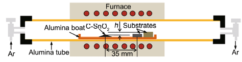
Silicon wafers (100) (Sigma-Aldrich) were used as substrates. The plates were ultrasonically cleaned in acetone, ethanol and distilled water for 30 min and then dried in nitrogen flow. A gold layer was sputter-coated on each plate using a sputter coater (BALZERS SCD 050) at 40 mA sputtering current, and its thickness was controlled by varying the sputtering time. A grinded mixture of graphite (Sigma-Aldrich, 99.99% purity, particle size <150 μm) and SnO2 powder (Sigma-Aldrich, 99.9% purity) (C/SnO2 = 3/5, in mol) was used as the evaporation source and loaded on a flat alumina boat locating at 35 mm far from the Si wafer (Fig. 1). The vertical distance between the powder and the gold layer (h in Fig. 1) was controlled by changing the height of the substrates. The growth of SnO2 was performed for 2 h at a temperature of 1000 °C. The source vapor of tin and tin oxide was produced through carbothermal process [17-19]. Pure argon at a flow rate of 100 cm3/min was used to carry the vapor to the growth sites.
Fig. 1 Schematic of the furnace system used for the synthesis of SnO2 nanowires
The structures of the produced samples were examined with SEM (Leica S440 tungsten filament and supra 55vp FEG-SEM) and XRD (X’Pert PRO). The contents of elements were tested by EDX (Leica S440 tungsten filament).
3 Results and Discussion
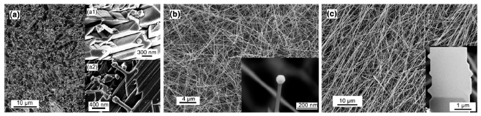
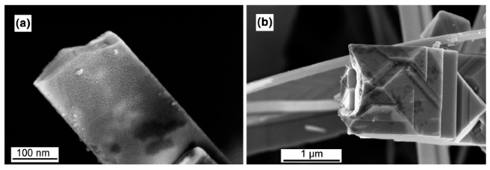
Heterostructure of tin dioxide was fabricated when the gold layer on a 0.5-mm height silicon wafer was controlled at about 25 nm in thickness, as shown in Fig. 2a. Vertical 1D nanowires grew on the top of the intricate nanowalls. It was observed that the nanowires were grown from the “rallying point” on the nanowalls as shown in Fig. 2a1. The nanowires are cylinder shape with a seed particle on the top. This suggests that the nanowires are the result of the epitaxial growth at the particles on the nanowalls surface. The growth is due to the interaction between the dynamic wetting behavior and the thermal-enhanced surface diffusion of gold adatoms on the substrates [20]. After the reaction period reduced to 2 h, particles formed on the top of the nanowalls were detected. They have quite different sizes from 100 to 200 nm in diameter. These particles came from the catalytic during the nanowall growth, so that with further reaction, nanowires grew from the sites and had a particle end, as shown in Fig. 2a2.
Fig. 2 SEM images of tin dioxides grown under different conditions: a SnO2 heterostructure grown on a substrate with 0.5 mm height and 25-nm gold layer, where inset a1 is for the nanowalls formed in 2 h and inset a2 is for nanowires grown after 2 h; b SnO2 nanowires grown on a substrate with 0.5 mm height and 12.5-nm gold layer, and the inset is the tip of the nanowires; c SnO2 whiskers grown on a substrate with 3 mm height and 12.5-nm gold layer, and the inset is the tip of the whiskers
Figure 2b shows tin dioxide nanowires produced on a 0.5-mm height silicon wafer with gold layer of 12.5 nm thickness of. Almost all of the nanowires have a round Au-Sn alloy particle on the top, as illustrated by the inset image. The dimension of the nanowires was approximately 50 nm, and the alloy catalytic was around 100 nm. The inset picture shows that the particulate tip of the nanowire is much brighter than the wire. This is because of the high content of gold in the tips and the edge effect in SEM technology. Figure 2c shows the whiskers obtained on a 3-mm height silicon wafer coated with 12.5-nm gold layer (the different gold heights on the substrate got the same result). The dimension of the whiskers is around 2 μm, and the tip is flat. Most of them had the same order as the evaporation flows inside of the tubular furnace from the inlet to the outlet. The experiments showed the that thickness of the gold layer has a critical impact on the morphology of SnO2 nanostructures.
It was found that the most import factor for heterostructure and nanowire growths is the thickness of the gold layer. Thin gold layer can easily aggregate to catalytic particles, so it is suitable for nanowires growth [21]. Thick gold layer will aggregate to large and non-uniform shapes, like belts, inducing the epitaxial growth of nanowalls. The catalyze layer on the top will reassemble during the nanowalls growth. After a reaction time, round catalyst drops form on the nanowalls as Fig. 2a illustrates. The catalyst drops can induce nanowire grown.
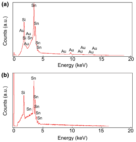
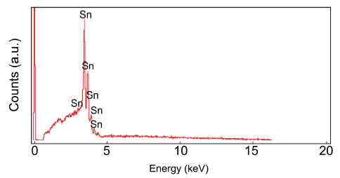
Most of the ends of the nanowires have a particle tip (Fig. 2a, b), which is a typical hemisphere or truncated sphere with a flat end on the top of the nanowires with a consistent diameter. EDX was performed on a nanowire tip and a nanowire body with point scan mode, and the results are shown in Fig. 3. It can be seen that the particle contains Sn and Au, while Sn is the only metallic element in the body part of nanowires. Although the quantities of C, N and O cannot be accurately measured by EDX, it is clear that the body of the nanowires contains more oxygen than the particle.
Fig. 3 EDX patterns of the seed part of nanowires a and the body of nanowires b; the peak of the silicon comes from the substrate
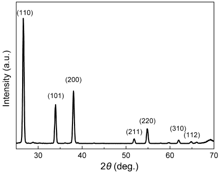
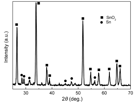
The crystallographic structure of the nanowires (Fig. 2b) was identified by XRD, as shown in Fig. 4. The three strong peaks of the XRD pattern are readily indexed to the tetragonal rutile structure of SnO2 with the lattice constants of a = b = 0.4737 and c = 0.3185 nm, which correspond with the data of cassiterite. Cassiterite is a kind of tin dioxide, which does not contain pure tin. In Fig. 4, it can be concluded that the nanowires are composed of SnO2 phase only, which confirms the afore-discussed mechanism of the nanowires growth.
According to the VLS mechanism, the Au-Sn alloy catalytic particles directly adsorb the source vapor. Based on the thermodynamic calculation of O-Sn system [18], SnO x has two formulates at 1000 °C and the main part is Sn-rich liquid phase containing Sn and SnO, and SnO is degenerated to Sn and SnO2 during cooling. So the source vapor is Sn rich and can solve into the alloy particles. After achieving saturation, Sn re-evaporates, while SnO2 precipitates to grow to nanowires. This explained the existence of oxygen in nanowires [19] and a lot of tin found in the outlet region of the tubular furnace.
It was found that the conditions, except the thickness of the gold layer, for the growth of heterostructure and nanowires of tin dioxide were the same. Therefore, the heterostructure growth is also through the VLS mechanism. The Au-Sn alloy is liquid phase at the experimental conditions used in the present work, which can be confirmed by Ref. [22]. A thin layer of the catalyst can easily aggregate to small particles, whereas a thick catalyst layer is more preferable to form belts for the growth of nanowalls (Fig. 2a). A mechanism for the formation of the intricate quasi-3D nanostructure is proposed in the present work, as illustrated in Fig. 5. The procedure is divided into three steps. In the first step, the gold layer coated on a substrate sorbs Sn vapor to form an Au-Sn liquid phase and shrinks to belt due to the tractive force of the surface tension and the poor interfacial wettability of the alloy on the substrate (Fig. 5a, b). The poor wettability can facilitate the formation of an Au network on the substrate at an elevated temperature [23]. During the second step, with the continuous supply of the source vapor by a gas carrier, SnO2 epitaxial growth is initiated at the narrow boundaries between the particulates formed by Au nanograins (Fig. 5b, c), because there are the most thermodynamically active sites for saturation and precipitation of the Au adatoms [23]. The surface energy at the rallying points increases with the diffusion and accumulation of Au atoms for overall energy compensation. In the meantime, the liquid alloy keeps shrinking and reduces in its amount, due to the evaporation and removal of some of the alloy by the gas flow at the high temperature. In the last step, the liquid alloy aggregates to particles. When Sn arrives its critical saturation point, 1D nanowires begin to grow from the rallying points via the same mechanism. Au nanoparticles are well dispersed on the top during the growth of 1D nanowires [24].
Fig. 5 Schematic diagrams for the growth of SnO2 nanowalls: a gold dropped on a substrate by sputter coating; b Au-Sn alloy belts formed through shirking at 1000 °C; c nanowalls grown from the “rallying points” and the alloy on the top gradually shirked to points for nanowire growth; d nanowires grown on the top of nanowalls
When a high substrate is applied, the source vapor tends to flow upward with the carrier gas and flow over the reaction area at a high concentration of the source [25]. The concentration of Sn vapor is higher than that of SnO in this area, which provides more Sn for the growth of nanostructures. It was found that whiskers could be fabricated when the substrate height is increased to 3 mm, which grew in the same direction (Fig. 2c). The whiskers have a flat end, and most of them have a dimension of about 2 μm in diameters. The cross section of the whiskers was characterized by SEM, as illustrated in Fig. 6, showing a Sn-SnO2 core-shell structure. The oxide shell covered the pure Sn degenerated from SnO in the middle. This structure was also fabricated in [26]. It was observed that the whiskers grew in the direction of precursor vapor flow.
Fig. 6 High magnification a and low magnification b SEM images of the cross sections of the whiskers
The XRD pattern of a whisker in Fig. 7 shows that there are two main constituents: tin dioxide and tin. This confirms the core-shell structure of whisker. The EDX result in Fig. 8 shows that the whisker consists of Sn and oxygen only, indicating there is no Au-Sn alloy participation during the wire growth. Thus, the formation of the whiskers is through the VS mechanism. Due to the high concentration of the source vapor, the whisker growth should be based on the self-assemble nucleation growth [26].
Fig. 8 EDX pattern scanned for full scale of a whisker specimen along its cross section
The partial pressure of Sn vapor at a low position in furnace, such as at the top of the 0.5-mm height substrate, is lower than that at the top of a high substrate [27]. The Sn solved into the alloy at the top of a low substrate is more easily gasified and removed by the argon. The nanowires grown on the low substrate only contain tin dioxide. At a high position, the concentration of Sn vapor is high enough for the growth of core-shell whiskers.
4 Conclusion
Various structures of tin dioxide were synthesized on silicon wafers through VLS and VS mechanisms. The thickness of the gold layer and the partial pressure of Sn vapor are the most important factors that control the structure of the products. Thin gold layer can form alloy points, whereas thick catalyst layer is preferable to aggregates nanobelts. The former rallying points lead to the growth of nanowires of tin dioxide and the latter points result in the growth of nanowalls, when a low-height substrate is used. Their growth was induced by Au-Sn alloy on VLS mechanism at a low concentration of sources vapor. The aggregated alloy partials or belts acted as catalysts for the growth of the tin dioxide nanowires and heterostructure. The partial pressure of source vapor at growing sites can be controlled by adjusting the height of substrate. High concentration of source vapor can be approached by increasing the substrate height and lead to the growth of whiskers. The whiskers with a core-shell (Sn-SnO2) structure were fabricated on a silicon substrate surface 3 mm high to the C-SnO2 powder.
Acknowledgments
This work was supported by Deakin University under a postgraduate research scholarship, the Fundamental Scientific Research Funds for Chinese Academy of Tropical Agricultural Sciences (Nos. 1630022011033 and 1630062013011) and the Natural Science Foundation of Hainan Province, China (No. 20155197).
The authors have declared that no competing interests exist.
... Tin dioxide (SnO2), as an important n-type semiconductor, has wide band gap (3.6 eV) and unique optical, electronic and photoelectrical properties [1, 2]. SnO2 has been widely used in various fields, for instance SnO2 thin films coated on glass as photocatalysts [3]; single generic tin oxide-based gas sensor for ethanol (gases) [4]; and free standing SnO2/reduced graphene oxide (RGO) nanocomposite for the anode of lithium-ion batteries [5]. With the rapid development of nano-manufacturing technology, one-dimensional [6-8] and hierarchical [9, 10] structures of SnO2 with attractive physical properties have been synthesized. The research has been focusing on the development of morphologically controlled SnO2 nanostructures through different methods, such as thermal evaporation, solution-based synthesis and template-assisted methods [11]. The thermal evaporation process is evaporating a stock and transferring to a substrate to form designed structure by using catalyst or through self-assembling process [12, 13]. Trung et al. [14] synthesized single-crystal SnO2 nanowires for NO x gas sensors by vapor-liquid-solid (VLS) method and the use of SiO2/Si catalyst. Amorin et al. [15] prepared SnO2 nanobelts for pH sensor by carbothermal method. Shen et al. [16] fabricated SnO2 nanorods by thermal evaporation of tin grains at 900 °C in argon-oxygen flow. Zhao et al. [10] used solution-based synthesis process in the fabrication of a hierarchical SnO2 nanosheet for lithium-ion battery. However, most of current researches focus on the manufacturing method for different morphologic structures, and few studies detailed the control of influencing factors for fabricating unique structures. ...
1
2014
... Tin dioxide (SnO2), as an important n-type semiconductor, has wide band gap (3.6 eV) and unique optical, electronic and photoelectrical properties [1, 2]. SnO2 has been widely used in various fields, for instance SnO2 thin films coated on glass as photocatalysts [3]; single generic tin oxide-based gas sensor for ethanol (gases) [4]; and free standing SnO2/reduced graphene oxide (RGO) nanocomposite for the anode of lithium-ion batteries [5]. With the rapid development of nano-manufacturing technology, one-dimensional [6-8] and hierarchical [9, 10] structures of SnO2 with attractive physical properties have been synthesized. The research has been focusing on the development of morphologically controlled SnO2 nanostructures through different methods, such as thermal evaporation, solution-based synthesis and template-assisted methods [11]. The thermal evaporation process is evaporating a stock and transferring to a substrate to form designed structure by using catalyst or through self-assembling process [12, 13]. Trung et al. [14] synthesized single-crystal SnO2 nanowires for NO x gas sensors by vapor-liquid-solid (VLS) method and the use of SiO2/Si catalyst. Amorin et al. [15] prepared SnO2 nanobelts for pH sensor by carbothermal method. Shen et al. [16] fabricated SnO2 nanorods by thermal evaporation of tin grains at 900 °C in argon-oxygen flow. Zhao et al. [10] used solution-based synthesis process in the fabrication of a hierarchical SnO2 nanosheet for lithium-ion battery. However, most of current researches focus on the manufacturing method for different morphologic structures, and few studies detailed the control of influencing factors for fabricating unique structures. ...
1
2012
... Tin dioxide (SnO2), as an important n-type semiconductor, has wide band gap (3.6 eV) and unique optical, electronic and photoelectrical properties [1, 2]. SnO2 has been widely used in various fields, for instance SnO2 thin films coated on glass as photocatalysts [3]; single generic tin oxide-based gas sensor for ethanol (gases) [4]; and free standing SnO2/reduced graphene oxide (RGO) nanocomposite for the anode of lithium-ion batteries [5]. With the rapid development of nano-manufacturing technology, one-dimensional [6-8] and hierarchical [9, 10] structures of SnO2 with attractive physical properties have been synthesized. The research has been focusing on the development of morphologically controlled SnO2 nanostructures through different methods, such as thermal evaporation, solution-based synthesis and template-assisted methods [11]. The thermal evaporation process is evaporating a stock and transferring to a substrate to form designed structure by using catalyst or through self-assembling process [12, 13]. Trung et al. [14] synthesized single-crystal SnO2 nanowires for NO x gas sensors by vapor-liquid-solid (VLS) method and the use of SiO2/Si catalyst. Amorin et al. [15] prepared SnO2 nanobelts for pH sensor by carbothermal method. Shen et al. [16] fabricated SnO2 nanorods by thermal evaporation of tin grains at 900 °C in argon-oxygen flow. Zhao et al. [10] used solution-based synthesis process in the fabrication of a hierarchical SnO2 nanosheet for lithium-ion battery. However, most of current researches focus on the manufacturing method for different morphologic structures, and few studies detailed the control of influencing factors for fabricating unique structures. ...
1
2014
... Tin dioxide (SnO2), as an important n-type semiconductor, has wide band gap (3.6 eV) and unique optical, electronic and photoelectrical properties [1, 2]. SnO2 has been widely used in various fields, for instance SnO2 thin films coated on glass as photocatalysts [3]; single generic tin oxide-based gas sensor for ethanol (gases) [4]; and free standing SnO2/reduced graphene oxide (RGO) nanocomposite for the anode of lithium-ion batteries [5]. With the rapid development of nano-manufacturing technology, one-dimensional [6-8] and hierarchical [9, 10] structures of SnO2 with attractive physical properties have been synthesized. The research has been focusing on the development of morphologically controlled SnO2 nanostructures through different methods, such as thermal evaporation, solution-based synthesis and template-assisted methods [11]. The thermal evaporation process is evaporating a stock and transferring to a substrate to form designed structure by using catalyst or through self-assembling process [12, 13]. Trung et al. [14] synthesized single-crystal SnO2 nanowires for NO x gas sensors by vapor-liquid-solid (VLS) method and the use of SiO2/Si catalyst. Amorin et al. [15] prepared SnO2 nanobelts for pH sensor by carbothermal method. Shen et al. [16] fabricated SnO2 nanorods by thermal evaporation of tin grains at 900 °C in argon-oxygen flow. Zhao et al. [10] used solution-based synthesis process in the fabrication of a hierarchical SnO2 nanosheet for lithium-ion battery. However, most of current researches focus on the manufacturing method for different morphologic structures, and few studies detailed the control of influencing factors for fabricating unique structures. ...
1
2012
... Tin dioxide (SnO2), as an important n-type semiconductor, has wide band gap (3.6 eV) and unique optical, electronic and photoelectrical properties [1, 2]. SnO2 has been widely used in various fields, for instance SnO2 thin films coated on glass as photocatalysts [3]; single generic tin oxide-based gas sensor for ethanol (gases) [4]; and free standing SnO2/reduced graphene oxide (RGO) nanocomposite for the anode of lithium-ion batteries [5]. With the rapid development of nano-manufacturing technology, one-dimensional [6-8] and hierarchical [9, 10] structures of SnO2 with attractive physical properties have been synthesized. The research has been focusing on the development of morphologically controlled SnO2 nanostructures through different methods, such as thermal evaporation, solution-based synthesis and template-assisted methods [11]. The thermal evaporation process is evaporating a stock and transferring to a substrate to form designed structure by using catalyst or through self-assembling process [12, 13]. Trung et al. [14] synthesized single-crystal SnO2 nanowires for NO x gas sensors by vapor-liquid-solid (VLS) method and the use of SiO2/Si catalyst. Amorin et al. [15] prepared SnO2 nanobelts for pH sensor by carbothermal method. Shen et al. [16] fabricated SnO2 nanorods by thermal evaporation of tin grains at 900 °C in argon-oxygen flow. Zhao et al. [10] used solution-based synthesis process in the fabrication of a hierarchical SnO2 nanosheet for lithium-ion battery. However, most of current researches focus on the manufacturing method for different morphologic structures, and few studies detailed the control of influencing factors for fabricating unique structures. ...
0
2009
1
2014
... Tin dioxide (SnO2), as an important n-type semiconductor, has wide band gap (3.6 eV) and unique optical, electronic and photoelectrical properties [1, 2]. SnO2 has been widely used in various fields, for instance SnO2 thin films coated on glass as photocatalysts [3]; single generic tin oxide-based gas sensor for ethanol (gases) [4]; and free standing SnO2/reduced graphene oxide (RGO) nanocomposite for the anode of lithium-ion batteries [5]. With the rapid development of nano-manufacturing technology, one-dimensional [6-8] and hierarchical [9, 10] structures of SnO2 with attractive physical properties have been synthesized. The research has been focusing on the development of morphologically controlled SnO2 nanostructures through different methods, such as thermal evaporation, solution-based synthesis and template-assisted methods [11]. The thermal evaporation process is evaporating a stock and transferring to a substrate to form designed structure by using catalyst or through self-assembling process [12, 13]. Trung et al. [14] synthesized single-crystal SnO2 nanowires for NO x gas sensors by vapor-liquid-solid (VLS) method and the use of SiO2/Si catalyst. Amorin et al. [15] prepared SnO2 nanobelts for pH sensor by carbothermal method. Shen et al. [16] fabricated SnO2 nanorods by thermal evaporation of tin grains at 900 °C in argon-oxygen flow. Zhao et al. [10] used solution-based synthesis process in the fabrication of a hierarchical SnO2 nanosheet for lithium-ion battery. However, most of current researches focus on the manufacturing method for different morphologic structures, and few studies detailed the control of influencing factors for fabricating unique structures. ...
1
2014
... Tin dioxide (SnO2), as an important n-type semiconductor, has wide band gap (3.6 eV) and unique optical, electronic and photoelectrical properties [1, 2]. SnO2 has been widely used in various fields, for instance SnO2 thin films coated on glass as photocatalysts [3]; single generic tin oxide-based gas sensor for ethanol (gases) [4]; and free standing SnO2/reduced graphene oxide (RGO) nanocomposite for the anode of lithium-ion batteries [5]. With the rapid development of nano-manufacturing technology, one-dimensional [6-8] and hierarchical [9, 10] structures of SnO2 with attractive physical properties have been synthesized. The research has been focusing on the development of morphologically controlled SnO2 nanostructures through different methods, such as thermal evaporation, solution-based synthesis and template-assisted methods [11]. The thermal evaporation process is evaporating a stock and transferring to a substrate to form designed structure by using catalyst or through self-assembling process [12, 13]. Trung et al. [14] synthesized single-crystal SnO2 nanowires for NO x gas sensors by vapor-liquid-solid (VLS) method and the use of SiO2/Si catalyst. Amorin et al. [15] prepared SnO2 nanobelts for pH sensor by carbothermal method. Shen et al. [16] fabricated SnO2 nanorods by thermal evaporation of tin grains at 900 °C in argon-oxygen flow. Zhao et al. [10] used solution-based synthesis process in the fabrication of a hierarchical SnO2 nanosheet for lithium-ion battery. However, most of current researches focus on the manufacturing method for different morphologic structures, and few studies detailed the control of influencing factors for fabricating unique structures. ...
2
2014
... Tin dioxide (SnO2), as an important n-type semiconductor, has wide band gap (3.6 eV) and unique optical, electronic and photoelectrical properties [1, 2]. SnO2 has been widely used in various fields, for instance SnO2 thin films coated on glass as photocatalysts [3]; single generic tin oxide-based gas sensor for ethanol (gases) [4]; and free standing SnO2/reduced graphene oxide (RGO) nanocomposite for the anode of lithium-ion batteries [5]. With the rapid development of nano-manufacturing technology, one-dimensional [6-8] and hierarchical [9, 10] structures of SnO2 with attractive physical properties have been synthesized. The research has been focusing on the development of morphologically controlled SnO2 nanostructures through different methods, such as thermal evaporation, solution-based synthesis and template-assisted methods [11]. The thermal evaporation process is evaporating a stock and transferring to a substrate to form designed structure by using catalyst or through self-assembling process [12, 13]. Trung et al. [14] synthesized single-crystal SnO2 nanowires for NO x gas sensors by vapor-liquid-solid (VLS) method and the use of SiO2/Si catalyst. Amorin et al. [15] prepared SnO2 nanobelts for pH sensor by carbothermal method. Shen et al. [16] fabricated SnO2 nanorods by thermal evaporation of tin grains at 900 °C in argon-oxygen flow. Zhao et al. [10] used solution-based synthesis process in the fabrication of a hierarchical SnO2 nanosheet for lithium-ion battery. However, most of current researches focus on the manufacturing method for different morphologic structures, and few studies detailed the control of influencing factors for fabricating unique structures. ...
... 10] used solution-based synthesis process in the fabrication of a hierarchical SnO2 nanosheet for lithium-ion battery. However, most of current researches focus on the manufacturing method for different morphologic structures, and few studies detailed the control of influencing factors for fabricating unique structures. ...
1
2013
... Tin dioxide (SnO2), as an important n-type semiconductor, has wide band gap (3.6 eV) and unique optical, electronic and photoelectrical properties [1, 2]. SnO2 has been widely used in various fields, for instance SnO2 thin films coated on glass as photocatalysts [3]; single generic tin oxide-based gas sensor for ethanol (gases) [4]; and free standing SnO2/reduced graphene oxide (RGO) nanocomposite for the anode of lithium-ion batteries [5]. With the rapid development of nano-manufacturing technology, one-dimensional [6-8] and hierarchical [9, 10] structures of SnO2 with attractive physical properties have been synthesized. The research has been focusing on the development of morphologically controlled SnO2 nanostructures through different methods, such as thermal evaporation, solution-based synthesis and template-assisted methods [11]. The thermal evaporation process is evaporating a stock and transferring to a substrate to form designed structure by using catalyst or through self-assembling process [12, 13]. Trung et al. [14] synthesized single-crystal SnO2 nanowires for NO x gas sensors by vapor-liquid-solid (VLS) method and the use of SiO2/Si catalyst. Amorin et al. [15] prepared SnO2 nanobelts for pH sensor by carbothermal method. Shen et al. [16] fabricated SnO2 nanorods by thermal evaporation of tin grains at 900 °C in argon-oxygen flow. Zhao et al. [10] used solution-based synthesis process in the fabrication of a hierarchical SnO2 nanosheet for lithium-ion battery. However, most of current researches focus on the manufacturing method for different morphologic structures, and few studies detailed the control of influencing factors for fabricating unique structures. ...
1
1996
... Tin dioxide (SnO2), as an important n-type semiconductor, has wide band gap (3.6 eV) and unique optical, electronic and photoelectrical properties [1, 2]. SnO2 has been widely used in various fields, for instance SnO2 thin films coated on glass as photocatalysts [3]; single generic tin oxide-based gas sensor for ethanol (gases) [4]; and free standing SnO2/reduced graphene oxide (RGO) nanocomposite for the anode of lithium-ion batteries [5]. With the rapid development of nano-manufacturing technology, one-dimensional [6-8] and hierarchical [9, 10] structures of SnO2 with attractive physical properties have been synthesized. The research has been focusing on the development of morphologically controlled SnO2 nanostructures through different methods, such as thermal evaporation, solution-based synthesis and template-assisted methods [11]. The thermal evaporation process is evaporating a stock and transferring to a substrate to form designed structure by using catalyst or through self-assembling process [12, 13]. Trung et al. [14] synthesized single-crystal SnO2 nanowires for NO x gas sensors by vapor-liquid-solid (VLS) method and the use of SiO2/Si catalyst. Amorin et al. [15] prepared SnO2 nanobelts for pH sensor by carbothermal method. Shen et al. [16] fabricated SnO2 nanorods by thermal evaporation of tin grains at 900 °C in argon-oxygen flow. Zhao et al. [10] used solution-based synthesis process in the fabrication of a hierarchical SnO2 nanosheet for lithium-ion battery. However, most of current researches focus on the manufacturing method for different morphologic structures, and few studies detailed the control of influencing factors for fabricating unique structures. ...
1
2011
... Tin dioxide (SnO2), as an important n-type semiconductor, has wide band gap (3.6 eV) and unique optical, electronic and photoelectrical properties [1, 2]. SnO2 has been widely used in various fields, for instance SnO2 thin films coated on glass as photocatalysts [3]; single generic tin oxide-based gas sensor for ethanol (gases) [4]; and free standing SnO2/reduced graphene oxide (RGO) nanocomposite for the anode of lithium-ion batteries [5]. With the rapid development of nano-manufacturing technology, one-dimensional [6-8] and hierarchical [9, 10] structures of SnO2 with attractive physical properties have been synthesized. The research has been focusing on the development of morphologically controlled SnO2 nanostructures through different methods, such as thermal evaporation, solution-based synthesis and template-assisted methods [11]. The thermal evaporation process is evaporating a stock and transferring to a substrate to form designed structure by using catalyst or through self-assembling process [12, 13]. Trung et al. [14] synthesized single-crystal SnO2 nanowires for NO x gas sensors by vapor-liquid-solid (VLS) method and the use of SiO2/Si catalyst. Amorin et al. [15] prepared SnO2 nanobelts for pH sensor by carbothermal method. Shen et al. [16] fabricated SnO2 nanorods by thermal evaporation of tin grains at 900 °C in argon-oxygen flow. Zhao et al. [10] used solution-based synthesis process in the fabrication of a hierarchical SnO2 nanosheet for lithium-ion battery. However, most of current researches focus on the manufacturing method for different morphologic structures, and few studies detailed the control of influencing factors for fabricating unique structures. ...
1
2012
... Tin dioxide (SnO2), as an important n-type semiconductor, has wide band gap (3.6 eV) and unique optical, electronic and photoelectrical properties [1, 2]. SnO2 has been widely used in various fields, for instance SnO2 thin films coated on glass as photocatalysts [3]; single generic tin oxide-based gas sensor for ethanol (gases) [4]; and free standing SnO2/reduced graphene oxide (RGO) nanocomposite for the anode of lithium-ion batteries [5]. With the rapid development of nano-manufacturing technology, one-dimensional [6-8] and hierarchical [9, 10] structures of SnO2 with attractive physical properties have been synthesized. The research has been focusing on the development of morphologically controlled SnO2 nanostructures through different methods, such as thermal evaporation, solution-based synthesis and template-assisted methods [11]. The thermal evaporation process is evaporating a stock and transferring to a substrate to form designed structure by using catalyst or through self-assembling process [12, 13]. Trung et al. [14] synthesized single-crystal SnO2 nanowires for NO x gas sensors by vapor-liquid-solid (VLS) method and the use of SiO2/Si catalyst. Amorin et al. [15] prepared SnO2 nanobelts for pH sensor by carbothermal method. Shen et al. [16] fabricated SnO2 nanorods by thermal evaporation of tin grains at 900 °C in argon-oxygen flow. Zhao et al. [10] used solution-based synthesis process in the fabrication of a hierarchical SnO2 nanosheet for lithium-ion battery. However, most of current researches focus on the manufacturing method for different morphologic structures, and few studies detailed the control of influencing factors for fabricating unique structures. ...
1
2014
... Tin dioxide (SnO2), as an important n-type semiconductor, has wide band gap (3.6 eV) and unique optical, electronic and photoelectrical properties [1, 2]. SnO2 has been widely used in various fields, for instance SnO2 thin films coated on glass as photocatalysts [3]; single generic tin oxide-based gas sensor for ethanol (gases) [4]; and free standing SnO2/reduced graphene oxide (RGO) nanocomposite for the anode of lithium-ion batteries [5]. With the rapid development of nano-manufacturing technology, one-dimensional [6-8] and hierarchical [9, 10] structures of SnO2 with attractive physical properties have been synthesized. The research has been focusing on the development of morphologically controlled SnO2 nanostructures through different methods, such as thermal evaporation, solution-based synthesis and template-assisted methods [11]. The thermal evaporation process is evaporating a stock and transferring to a substrate to form designed structure by using catalyst or through self-assembling process [12, 13]. Trung et al. [14] synthesized single-crystal SnO2 nanowires for NO x gas sensors by vapor-liquid-solid (VLS) method and the use of SiO2/Si catalyst. Amorin et al. [15] prepared SnO2 nanobelts for pH sensor by carbothermal method. Shen et al. [16] fabricated SnO2 nanorods by thermal evaporation of tin grains at 900 °C in argon-oxygen flow. Zhao et al. [10] used solution-based synthesis process in the fabrication of a hierarchical SnO2 nanosheet for lithium-ion battery. However, most of current researches focus on the manufacturing method for different morphologic structures, and few studies detailed the control of influencing factors for fabricating unique structures. ...
1
2011
... Silicon wafers (100) (Sigma-Aldrich) were used as substrates. The plates were ultrasonically cleaned in acetone, ethanol and distilled water for 30 min and then dried in nitrogen flow. A gold layer was sputter-coated on each plate using a sputter coater (BALZERS SCD 050) at 40 mA sputtering current, and its thickness was controlled by varying the sputtering time. A grinded mixture of graphite (Sigma-Aldrich, 99.99% purity, particle size <150 μm) and SnO2 powder (Sigma-Aldrich, 99.9% purity) (C/SnO2 = 3/5, in mol) was used as the evaporation source and loaded on a flat alumina boat locating at 35 mm far from the Si wafer (Fig. 1). The vertical distance between the powder and the gold layer (h in Fig. 1) was controlled by changing the height of the substrates. The growth of SnO2 was performed for 2 h at a temperature of 1000 °C. The source vapor of tin and tin oxide was produced through carbothermal process [17-19]. Pure argon at a flow rate of 100 cm3/min was used to carry the vapor to the growth sites. ...
1
2003
... According to the VLS mechanism, the Au-Sn alloy catalytic particles directly adsorb the source vapor. Based on the thermodynamic calculation of O-Sn system [18], SnO x has two formulates at 1000 °C and the main part is Sn-rich liquid phase containing Sn and SnO, and SnO is degenerated to Sn and SnO2 during cooling. So the source vapor is Sn rich and can solve into the alloy particles. After achieving saturation, Sn re-evaporates, while SnO2 precipitates to grow to nanowires. This explained the existence of oxygen in nanowires [19] and a lot of tin found in the outlet region of the tubular furnace. ...
2
2006
... Silicon wafers (100) (Sigma-Aldrich) were used as substrates. The plates were ultrasonically cleaned in acetone, ethanol and distilled water for 30 min and then dried in nitrogen flow. A gold layer was sputter-coated on each plate using a sputter coater (BALZERS SCD 050) at 40 mA sputtering current, and its thickness was controlled by varying the sputtering time. A grinded mixture of graphite (Sigma-Aldrich, 99.99% purity, particle size <150 μm) and SnO2 powder (Sigma-Aldrich, 99.9% purity) (C/SnO2 = 3/5, in mol) was used as the evaporation source and loaded on a flat alumina boat locating at 35 mm far from the Si wafer (Fig. 1). The vertical distance between the powder and the gold layer (h in Fig. 1) was controlled by changing the height of the substrates. The growth of SnO2 was performed for 2 h at a temperature of 1000 °C. The source vapor of tin and tin oxide was produced through carbothermal process [17-19]. Pure argon at a flow rate of 100 cm3/min was used to carry the vapor to the growth sites. ...
... According to the VLS mechanism, the Au-Sn alloy catalytic particles directly adsorb the source vapor. Based on the thermodynamic calculation of O-Sn system [18], SnO x has two formulates at 1000 °C and the main part is Sn-rich liquid phase containing Sn and SnO, and SnO is degenerated to Sn and SnO2 during cooling. So the source vapor is Sn rich and can solve into the alloy particles. After achieving saturation, Sn re-evaporates, while SnO2 precipitates to grow to nanowires. This explained the existence of oxygen in nanowires [19] and a lot of tin found in the outlet region of the tubular furnace. ...
1
2007
... Heterostructure of tin dioxide was fabricated when the gold layer on a 0.5-mm height silicon wafer was controlled at about 25 nm in thickness, as shown in Fig. 2a. Vertical 1D nanowires grew on the top of the intricate nanowalls. It was observed that the nanowires were grown from the “rallying point” on the nanowalls as shown in Fig. 2a1. The nanowires are cylinder shape with a seed particle on the top. This suggests that the nanowires are the result of the epitaxial growth at the particles on the nanowalls surface. The growth is due to the interaction between the dynamic wetting behavior and the thermal-enhanced surface diffusion of gold adatoms on the substrates [20]. After the reaction period reduced to 2 h, particles formed on the top of the nanowalls were detected. They have quite different sizes from 100 to 200 nm in diameter. These particles came from the catalytic during the nanowall growth, so that with further reaction, nanowires grew from the sites and had a particle end, as shown in Fig. 2a2. ...
1
2006
... It was found that the most import factor for heterostructure and nanowire growths is the thickness of the gold layer. Thin gold layer can easily aggregate to catalytic particles, so it is suitable for nanowires growth [21]. Thick gold layer will aggregate to large and non-uniform shapes, like belts, inducing the epitaxial growth of nanowalls. The catalyze layer on the top will reassemble during the nanowalls growth. After a reaction time, round catalyst drops form on the nanowalls as Fig. 2a illustrates. The catalyst drops can induce nanowire grown. ...
1
2007
... It was found that the conditions, except the thickness of the gold layer, for the growth of heterostructure and nanowires of tin dioxide were the same. Therefore, the heterostructure growth is also through the VLS mechanism. The Au-Sn alloy is liquid phase at the experimental conditions used in the present work, which can be confirmed by Ref. [22]. A thin layer of the catalyst can easily aggregate to small particles, whereas a thick catalyst layer is more preferable to form belts for the growth of nanowalls (Fig. 2a). A mechanism for the formation of the intricate quasi-3D nanostructure is proposed in the present work, as illustrated in Fig. 5. The procedure is divided into three steps. In the first step, the gold layer coated on a substrate sorbs Sn vapor to form an Au-Sn liquid phase and shrinks to belt due to the tractive force of the surface tension and the poor interfacial wettability of the alloy on the substrate (Fig. 5a, b). The poor wettability can facilitate the formation of an Au network on the substrate at an elevated temperature [23]. During the second step, with the continuous supply of the source vapor by a gas carrier, SnO2 epitaxial growth is initiated at the narrow boundaries between the particulates formed by Au nanograins (Fig. 5b, c), because there are the most thermodynamically active sites for saturation and precipitation of the Au adatoms [23]. The surface energy at the rallying points increases with the diffusion and accumulation of Au atoms for overall energy compensation. In the meantime, the liquid alloy keeps shrinking and reduces in its amount, due to the evaporation and removal of some of the alloy by the gas flow at the high temperature. In the last step, the liquid alloy aggregates to particles. When Sn arrives its critical saturation point, 1D nanowires begin to grow from the rallying points via the same mechanism. Au nanoparticles are well dispersed on the top during the growth of 1D nanowires [24]. ...
2
2003
... It was found that the conditions, except the thickness of the gold layer, for the growth of heterostructure and nanowires of tin dioxide were the same. Therefore, the heterostructure growth is also through the VLS mechanism. The Au-Sn alloy is liquid phase at the experimental conditions used in the present work, which can be confirmed by Ref. [22]. A thin layer of the catalyst can easily aggregate to small particles, whereas a thick catalyst layer is more preferable to form belts for the growth of nanowalls (Fig. 2a). A mechanism for the formation of the intricate quasi-3D nanostructure is proposed in the present work, as illustrated in Fig. 5. The procedure is divided into three steps. In the first step, the gold layer coated on a substrate sorbs Sn vapor to form an Au-Sn liquid phase and shrinks to belt due to the tractive force of the surface tension and the poor interfacial wettability of the alloy on the substrate (Fig. 5a, b). The poor wettability can facilitate the formation of an Au network on the substrate at an elevated temperature [23]. During the second step, with the continuous supply of the source vapor by a gas carrier, SnO2 epitaxial growth is initiated at the narrow boundaries between the particulates formed by Au nanograins (Fig. 5b, c), because there are the most thermodynamically active sites for saturation and precipitation of the Au adatoms [23]. The surface energy at the rallying points increases with the diffusion and accumulation of Au atoms for overall energy compensation. In the meantime, the liquid alloy keeps shrinking and reduces in its amount, due to the evaporation and removal of some of the alloy by the gas flow at the high temperature. In the last step, the liquid alloy aggregates to particles. When Sn arrives its critical saturation point, 1D nanowires begin to grow from the rallying points via the same mechanism. Au nanoparticles are well dispersed on the top during the growth of 1D nanowires [24]. ...
... 23]. The surface energy at the rallying points increases with the diffusion and accumulation of Au atoms for overall energy compensation. In the meantime, the liquid alloy keeps shrinking and reduces in its amount, due to the evaporation and removal of some of the alloy by the gas flow at the high temperature. In the last step, the liquid alloy aggregates to particles. When Sn arrives its critical saturation point, 1D nanowires begin to grow from the rallying points via the same mechanism. Au nanoparticles are well dispersed on the top during the growth of 1D nanowires [24]. ...
1
2013
... It was found that the conditions, except the thickness of the gold layer, for the growth of heterostructure and nanowires of tin dioxide were the same. Therefore, the heterostructure growth is also through the VLS mechanism. The Au-Sn alloy is liquid phase at the experimental conditions used in the present work, which can be confirmed by Ref. [22]. A thin layer of the catalyst can easily aggregate to small particles, whereas a thick catalyst layer is more preferable to form belts for the growth of nanowalls (Fig. 2a). A mechanism for the formation of the intricate quasi-3D nanostructure is proposed in the present work, as illustrated in Fig. 5. The procedure is divided into three steps. In the first step, the gold layer coated on a substrate sorbs Sn vapor to form an Au-Sn liquid phase and shrinks to belt due to the tractive force of the surface tension and the poor interfacial wettability of the alloy on the substrate (Fig. 5a, b). The poor wettability can facilitate the formation of an Au network on the substrate at an elevated temperature [23]. During the second step, with the continuous supply of the source vapor by a gas carrier, SnO2 epitaxial growth is initiated at the narrow boundaries between the particulates formed by Au nanograins (Fig. 5b, c), because there are the most thermodynamically active sites for saturation and precipitation of the Au adatoms [23]. The surface energy at the rallying points increases with the diffusion and accumulation of Au atoms for overall energy compensation. In the meantime, the liquid alloy keeps shrinking and reduces in its amount, due to the evaporation and removal of some of the alloy by the gas flow at the high temperature. In the last step, the liquid alloy aggregates to particles. When Sn arrives its critical saturation point, 1D nanowires begin to grow from the rallying points via the same mechanism. Au nanoparticles are well dispersed on the top during the growth of 1D nanowires [24]. ...
1
2013
... When a high substrate is applied, the source vapor tends to flow upward with the carrier gas and flow over the reaction area at a high concentration of the source [25]. The concentration of Sn vapor is higher than that of SnO in this area, which provides more Sn for the growth of nanostructures. It was found that whiskers could be fabricated when the substrate height is increased to 3 mm, which grew in the same direction (Fig. 2c). The whiskers have a flat end, and most of them have a dimension of about 2 μm in diameters. The cross section of the whiskers was characterized by SEM, as illustrated in Fig. 6, showing a Sn-SnO2 core-shell structure. The oxide shell covered the pure Sn degenerated from SnO in the middle. This structure was also fabricated in [26]. It was observed that the whiskers grew in the direction of precursor vapor flow. ...
2
2006
... When a high substrate is applied, the source vapor tends to flow upward with the carrier gas and flow over the reaction area at a high concentration of the source [25]. The concentration of Sn vapor is higher than that of SnO in this area, which provides more Sn for the growth of nanostructures. It was found that whiskers could be fabricated when the substrate height is increased to 3 mm, which grew in the same direction (Fig. 2c). The whiskers have a flat end, and most of them have a dimension of about 2 μm in diameters. The cross section of the whiskers was characterized by SEM, as illustrated in Fig. 6, showing a Sn-SnO2 core-shell structure. The oxide shell covered the pure Sn degenerated from SnO in the middle. This structure was also fabricated in [26]. It was observed that the whiskers grew in the direction of precursor vapor flow. ...
... The XRD pattern of a whisker in Fig. 7 shows that there are two main constituents: tin dioxide and tin. This confirms the core-shell structure of whisker. The EDX result in Fig. 8 shows that the whisker consists of Sn and oxygen only, indicating there is no Au-Sn alloy participation during the wire growth. Thus, the formation of the whiskers is through the VS mechanism. Due to the high concentration of the source vapor, the whisker growth should be based on the self-assemble nucleation growth [26]. ...
1
2010
... The partial pressure of Sn vapor at a low position in furnace, such as at the top of the 0.5-mm height substrate, is lower than that at the top of a high substrate [27]. The Sn solved into the alloy at the top of a low substrate is more easily gasified and removed by the argon. The nanowires grown on the low substrate only contain tin dioxide. At a high position, the concentration of Sn vapor is high enough for the growth of core-shell whiskers. ...
 , Peter Hodgson
 WeChat
