

Effect of Annealing on the Microstructure and Properties of In-situ Cu-Nb Microcomposite Wires
[Li-Ping Deng1  , Bing-Shu Wang
1 , Hong-Liang Xiang1 , Xiao-Fang Yang2 , Rong-Mei Niu3 , Ke Han3 ]
, Bing-Shu Wang]
|
|


The effects of annealing on microstructure, magnetoresistance, and hardness of an in situ Cu-Nb microcomposite wire have been investigated. Neither changes in microstructure nor hardness were found until 500 °C. Particularly, microstructural change within the Nb films was observed in the annealed samples. The room-temperature magnetoresistivity was almost negligible, while magnetoresistivity at -196 °C increased with magnetic field. At temperature above 500 °C, recovery and recrystallization occurred, and both the resistance and hardness decreased.
Cu-Nb microcomposite wires have drawn wide attention due to their good combination of high mechanical strength and electrical conductivity, thus making them be a good candidate for winding of high-field pulsed magnets [1, 2, 3, 4, 5]. Magnetoresistance (MR) is the change in resistivity of the materials induced by the interaction of magnetic field with conductive electrons in materials. In metal-metal composite, MR may be affected by the densities of interfaces, and it can be expressed by Kohler’ s rule [6, 7]:
$${\text{MR}} = \frac{\Delta \rho }{{\rho_{0} }} = \frac{\rho (B, T) - \rho (0, T)}{\rho (0, T)}, $$
where ρ (B, T) and ρ (0, T) are the resistivity values of the specimen measured at temperature T with and without magnetic field B, respectively. ρ 0 is the resistivity value at zero magnetic field.
In most application conditions, the wires are exposed to Joule heating due to electrical resistance [1, 8], which induces obviously changes in the microstructure and properties of Cu-Nb composite wires, such as the spheroidization and coarsening of Nb phases, the decrease in the mechanical strength, and the increase in the electrical conductivity. These will affect the service life of the wires and, consequently, the magnet [9, 10, 11, 12, 13, 14]. Therefore, it is desirable to understand the microstructure, strength, and MR responses to heat treatment at different temperatures.
The electrical resistance of Cu-Nb microcomposites without magnetic field at both as-deformed and annealed states has been studied extensively [15, 16, 17, 18, 19, 20]. The resistance increases when the microstructural size of the specimen is reduced into the levels comparable with the mean free path of electrons in the matrix. In this case, the electron scattering by the interfaces is considered as the major source for the increased resistivity [6, 8, 21]. Verhoeven et al. [15] found that the resistivity of heavily drawn Cu-Nb wire without magnetic fields was mainly contributed to the electron scattering at Cu-Nb interfaces, and the increase in electrical conductivity after annealing was due to both Nb filament coarsening and dislocation annihilation. Our previous study [20] showed that the resistivity raised as the interface area density increased. However, unlike electrical resistance at zero magnetic field, or the MR of Cu-Ag composites [22, 23] or pure metals [24, 25, 26, 27, 28], the electrical resistance of Cu-Nb composites with a magnetic field (MR) has not been widely studied, and there are few reports focusing upon the MR of Cu-Nb microcomposite wires before or after annealing. Electrical resistance in magnetic field is an important property needed to safely survive the harsh operating conditions in magnets. Yet now only few data on MR of Cu-Nb composites at magnetic fields are available in the reported literatures. Nick et al. [29] stated that the MR of Cu-Nb at low-field strength (below 0.6 T) was small because of the relatively low residual resistivity ratio. Heringhaus et al. [11] reported the dependence of resistivity on magnetic field strength up to 15 T and found that the resistivity of deformed Cu-Nb wires changed marginally until the magnetic field reached 4 T.
High magnetic field has received significant attention, and the performance of materials under high magnetic field can be further enhanced performance [30]. Thus, it is necessary to extend the range of MR measurement at higher field at both room temperature (RT) and -196 ° C, and this is useful for better understanding the relationship between the microstructure and resistivity properties, in order to design the next generation composite conductors.
Microhardness tests are often used to evaluate the mechanical strength of small specimens because the indentations can be made very small and nondestructive (or semi-destructive) [31]. In this paper, the microstructure evolution, MR, and microhardness of in situ Cu-Nb microcomposite wires both before and after annealing were investigated. The influence of the microstructure changes on MR and hardness was analyzed and discussed.
The specimens used in this study are in situ Cu-Nb microcomposite wires with a diameter of 0.16 mm and a strain of 10.1. The detailed wire fabrication process can be found in our previous paper [20]. The specimens were cut from the wire and sealed, respectively, in 6 quartz tubes with the vacuum of about 10-3 Pa, followed by annealing at temperatures from 400 to 900 ° C for 1 h in the center of furnace, respectively, and the temperature interval was 100 ° C.
The specimens for scanning electron microscopy (SEM) were etched with a solution of 20% nitric acid in 80% deionized water. The cross-sectional and longitudinal sectional microstructures of the specimens were investigated by Zeiss 1540XB scanning microscope and Zeiss Supra 55 scanning microscope at an accelerating voltage of 15 kV.
The specimens at both drawn and annealed states were investigated in magnetic field at RT (about 25 ° C) as well as -196 ° C. MR of the specimens was measured by a standard four-probe method with a bore of 195 mm diameter and a resistive high magnetic field up to 19.1 T. The specimens were fixed on a holder which was immersed in liquid nitrogen and centered in the magnet bore. The measured temperature was monitored by a sensor, and the temperature measured was (-196 ± 2) ° C. An gradual buildup of excitation current up to 1 A was generated by a Keithly 2400 current source, and the voltage was measured by a Keithly 2012 multimeter. The magnetic flux density was perpendicular to both the wire axis and current direction as shown in Fig. 1. The distance between the voltage taps was about 90 mm.
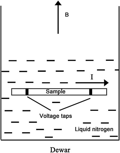 | Fig. 1 Experimental setup for MR test. B is the external magnetic field; I is the current |
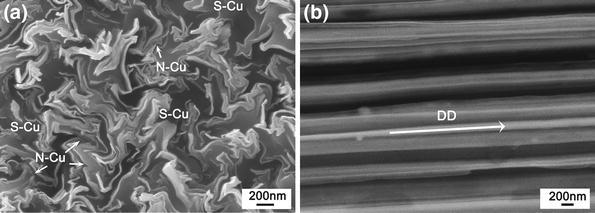
In Fig. 2, both the cross-sectional and longitudinal SEM images of drawn Cu-Nb microcomposite wires show Cu matrix in dark regions and Nb phases in light regions. Nb phase is highly curling on cross section (Fig. 2a), and highly aligned and elongated along the drawing direction (DD) (Fig. 2b). They are (25 ± 5) nm thick and (1036 ± 20) nm wide, giving an aspect ratio of around 41.4. The aspect ratio is defined by w/t, where w is the width of the ribbon and t is the thickness. Thus, the Nb phase exhibits a thin ribbon shape on the longitudinal section and can be treated as finite thin films, since the ratio is much higher than 10 in the work by Sandim et al. [1].
 | Fig. 2 SEM images showing the microstructures of as-drawn wires: a cross section; b longitudinal section. The arrow shows the drawing direction or the wire axis |
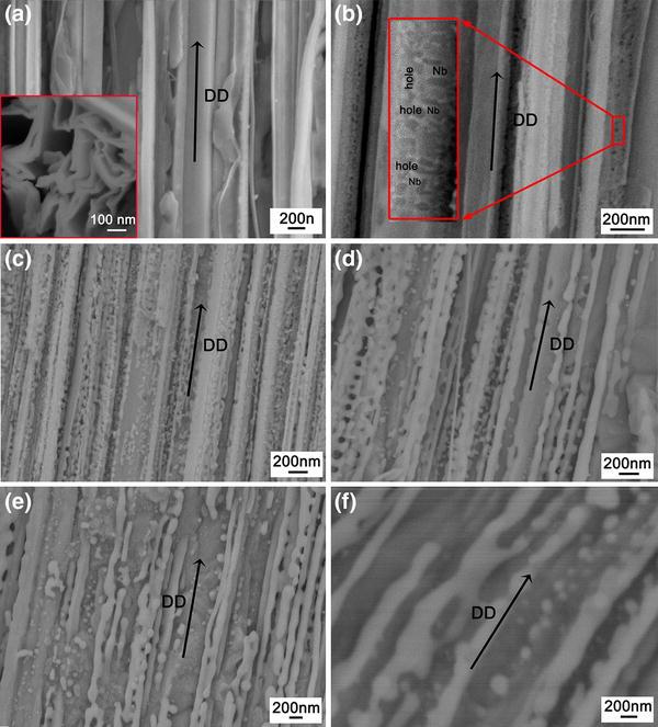
Annealing at different temperatures provides different microstructures (Fig. 3). At 400 ° C or below (Fig. 3a), both the edge and surface of each Nb ribbon/film are well defined, as shown in the inset in Fig. 3a. It preserves a severe curling shape on cross section and around 25 nm in thickness, indicating that no obvious changes occurred during the heat treatment. The broke up of Nb films shown in Fig. 3a is mainly attributed to the removal of Cu matrix and ultrasonic cleaning during specimen preparation. As shown in Fig. 3b, a number of small holes/pits form within Nb films after annealing at 500 ° C. This phenomenon is different from those of the reports [1, 32, 33, 34], most of whom found the boundary splitting and groove formation along the boundaries after annealing [1, 35]. Sharma et al. [10] presented several major models for the coarsening of Nb including direct cylinderization, edge spheroidization, termination migration, discontinuous coarsening, and boundary splitting. None of these models depict the microstructure changes deriving from the wide surface of Nb thin ribbon/films. The coarsening of Nb in the present work is believed to derive from the regions with certain low-angle misorientations within Nb films, where elastic energy carried by the stress was built during the wire drawing process. Diffusion of Nb atoms from these strained regions to less-strain regions took place during annealing [36, 37], resulting in the formation of the grooves and pits as observed in this study. Besides, the curvature of Nb film is believed to provide a driving force for particle migration and coalescence within Nb films. At higher temperatures (Fig. 3c-f), recrystallization, spheroidization, and coarsening occurred, even Nb precipitation might take place [38, 39], affecting the magnetoresistance and hardness of the wires. Details for the microstructural changes will be addressed in another paper.
 | Fig. 3 Longitudinal microstructures of Cu-Nb microcomposite wires after annealing at different temperatures for 1 h: a 400 ° C, the inset showing the cross-sectional image, b 500 ° C, c 600 ° C, d 700 ° C, e 800 ° C, f 900 ° C; the arrows showing drawing direction (DD) or the wire axis |
Table 1 presents the sizes of Cu and Nb phases and the mean free paths (lo) of electrons in two phases at 25 and -196 ° C. We can see that after annealing at 400 ° C, the sizes are almost unchanged which are about 25 nm for Nb and 55 nm for Cu, indicating no recrystallization occurred during the annealing, while annealing at 900 ° C both appeared obvious recrystallization followed by coarsening of Nb and Cu phase. This is coincident with the results in Fig. 3.
| Table 1 Microstructural sizes of Nb and Cu phases (Nb phase in thickness or diameter, Cu phase in width, and electron mean free path lo) |
A large number of small Nb particles can also be observed in Fig. 3e and f, which provide large density of the phase boundaries. These small Nb particles in annealed wires are expected to be precipitates either due to large interface curvature and internal stress during wire fabrication [20] or Ostwald ripening where small particles form to decrease elastic energy [41]. More discussion will be addressed in the future.
The effect of the magnet field strength on the resistivity of the Cu-Nb composites is shown in Fig. 4. It can be seen that at RT (25 ° C), the effect of the magnetic field on the resistance of the specimens is fairly small. The MR values are only a few percent (less than 5%), even at 19.1 T, as shown in Fig. 4a. These slight variations can be negligible.
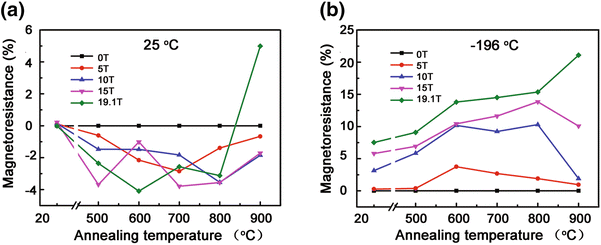 | Fig. 4 MR of wires plotted as annealing temperatures: a tested at 25 ° C; b tested at -196 ° C. The annealing temperature for the as-drawn specimen is assumed to be 25 ° C |
Annealing states at 25 and 400 ° C, both the Cu sizes are comparable with lo. This is the case where the resistivity is expected to increase and the scattering by the interfaces, and it is considered as the major source for the increased resistivity [6, 8, 11]. The MR at -196 ° C (Fig. 4b) shows no significant change up to a magnetic field of 5 T, where the Lorentz force is not sufficient for notable change in resistance, particularly for the wires annealed at temperatures below 500 ° C. This is attributed to the delay of recovery and recrystallization in Cu matrix by well-defined and high density of Cu-Nb interfaces [42, 43]. At higher fields, the Lorentz force is sufficiently high to force the electrons to change their direction from straight lines to helical paths, and thus reduces the path length they can travel before they are scattered by the grain boundaries or interfaces [44]. This leads to increase in MR. The MR of the wires annealed at 900 ° C can reach 22% at a field of 19.1 T (Fig. 4b).
At temperatures below 800 ° C (Fig. 4b), the MR increases with the annealing temperature. This may be due to the small Nb particles observed in these annealed wires. However, the MR decreases notably in the wire annealed at 900 ° C in 10 and 15 T (Fig. 4b). This decline is owed to the decrease in surface area and dislocation scattering by spheroidization and coarsening at 900 ° C annealing [6, 45].
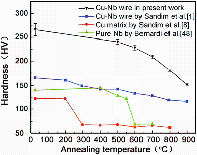
The evolution of the microhardness before and after annealing is shown in Fig. 5. Data from some reports are also presented in Fig. 5 for comparison. It can be seen that the hardness values in present work show minor decrease at temperatures below 500 ° C, which is possibly attributed to the recovery and recrystallization of the submicro-Cu matrix (S-Cu) [42, 46] (Fig. 2a). After annealing at temperatures above 500 ° C, more drops in hardness can be observed, while the hardness obtained by Sandim et al. (blue line in Fig. 5) shows almost linear drop, which is possibly due to the larger scale of their microstructure, and the hardness of Cu matrix dropped at around 200 ° C as expected (red line in Fig. 5) [8]. Our previous study found that the lattice relaxation, recovery, and crystal rotation in Cu matrix could be suppressed by high density of interfaces, which interacted with dislocations and precipitate strengthening component of the wires [4, 47]. The microstructure did not change until the wires were annealed at 500 ° C. At temperatures over 600 ° C, the hardness of Nb drops dramatically as a result of recovery and recrystallization of Nb (green line in Fig. 5) [48]. Therefore, the minor drop at temperatures below 500 ° C is mainly due to the recovery and recrystallization of S-Cu, while the sharp drop in hardness at temperatures above 500 ° C is primarily attributed to the perforation, necking, and spheroidization of Nb ribbon/films. Furthermore, annealing, on one hand, decreases the hardness by reducing the lattice defects formed during drawing; on the other hand, it may introduce small Nb particles to reduce elastic energy, as described above, inducing lattice distortion and, consequently, leading to solid solution hardening [20]. Thus, two mechanisms, solid solution hardening and annealing softening, should be considered for mechanical property analysis during annealing process. In our wires, the sharp drop in Fig. 5 shows that the softening outdoes the solution hardening, and the change of Nb from films/ribbon to bamboo/rod in shape in Fig. 3 induces severe decrease in hardness, making softening be the dominate mechanism during high-temperature annealing.
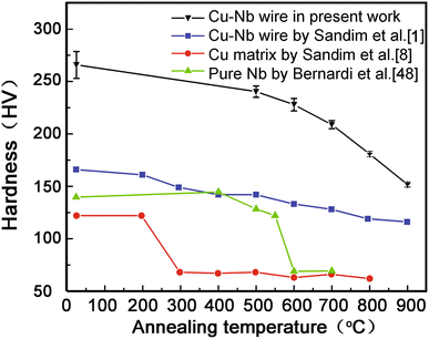 | Fig. 5 Hardness response after annealing |
This paper reports the microstructure evolution during annealing and its effect on the magnetoresistance and hardness of Cu-Nb composite wires. The results reveal that both the microstructure and hardness do not change obviously until annealing temperatures up to 500 ° C, showing the composite to be high thermal stability. The microstructure change in Nb is found to derive from within Nb films, and it is suggested to concern in the orientation variation. The room-temperature MR is marginal up to 19.1 T, while MR at -196 ° C exhibits distinct change and it reaches 22% at 19.1 T. This work suggests that the annealing below 500 ° C can be used to preserve both the hardness and MR, and annealing softening is proposed to be a domination mechanism of the property at elevated temperatures.
Acknowledgments:This research was funded by the National Natural Science Foundation of China (Grant Nos. 51421001 and 51301040), the Natural Science Foundation of Fujian Province of China (No. 2016J05119), and the Science and Technology Fund from Fujian Education Department of China (Grant No. JA15072). A portion of this work was performed at the National High Magnetic Field Laboratory, which is supported by US National Science Foundation Cooperative Agreement No. DMR-1157490 and the State of Florida. The authors are grateful for the kind support from Dr. Jun Lu, Dr. Yifeng Su, Dr. Lei Qu, and Dr. Xiaowei Zuo for their great help during the tests.
The authors have declared that no competing interests exist.
| [1] |
|
| [2] |
|
| [3] |
|
| [4] |
|
| [5] |
|
| [6] |
|
| [7] |
|
| [8] |
|
| [9] |
|
| [10] |
|
| [11] |
|
| [12] |
|
| [13] |
|
| [14] |
|
| [15] |
|
| [16] |
|
| [17] |
|
| [18] |
|
| [19] |
|
| [20] |
|
| [21] |
|
| [22] |
|
| [23] |
|
| [24] |
|
| [25] |
|
| [26] |
|
| [27] |
|
| [28] |
|
| [29] |
|
| [30] |
|
| [31] |
|
| [32] |
|
| [33] |
|
| [34] |
|
| [35] |
|
| [36] |
|
| [37] |
|
| [38] |
|
| [39] |
|
| [40] |
|
| [41] |
|
| [42] |
|
| [43] |
|
| [44] |
|
| [45] |
|
| [46] |
|
| [47] |
|
| [48] |
|