Growth and Characterization of Pencil-Like ZnO Nanowires in the Presence of a Disturbance in Boundary Layer
[A. Kamalianfar1, 2  , Mahmoud Godarz Naseri
3 , Marzih Kamalianfar2 , S. A. Halim4 , K. P. Lim4 ]
, Mahmoud Godarz Naseri|
|


Pencil-like zinc oxide (ZnO) nanowire was synthesized on Si (111) substrate through a simple vapor phase method using a mixture of zinc oxide and graphite as the source material. The source inside a quartz tube created a Zn-rich vapor that facilitated the formation and growth of ZnO nanowires. Field emission scanning electron microscopic studies indicated that pencil-like ZnO nanowires had a size of the range from 50 to 150 nm in diameter and several microns in length. X-ray diffraction was used to investigate the crystal structure of ZnO nanowires. Raman scattering and photoluminescence were applied to characterize the optical properties of the pencils. The growth mechanism of the nanopencils was discussed based on the growth conditions.
Zinc oxide (ZnO) with a direct band gap of 3.37 eV and large exciton binding energy of 60 meV at room temperature (RT) is a promising material for many applications in electronic and optical wave guide devices such as solar cells, gas sensor ultraviolet (UV) light-emitting devices and so on.
In recent years, fabrication and characterization of ZnO micro- and nanostructures have attracted remarkable attention due to their outstanding structure- and size-dependent optical and electrical properties [1, 2, 3, 4]. Because the properties of materials depend much on their sizes and shapes, it is necessary to study various sizes and morphographies of ZnO nanostructures.
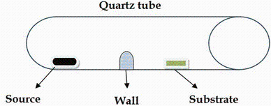
The controlled synthesis of the nanostructures, which is incorporated into functional nanodevices, is a rather challenging issue for desired size, shape, and orientation. One way to solve this problem is to synthesize various nanostructures by various methods. The growth of ZnO nanostructures has been reported by various methods, including hydrothermal process [5], laser ablation [6] vapor phase methods [7, 8], and sol-gel [9]. Most of modifications in the basic system geometry aim to allow for better control of the reaction conditions in the vapor phase. Accordingly, in the present work, we demonstrate a simple approach to synthesizing ZnO nanowires using a vapor-phase transport method under air atmosphere to reduce energy consumption. In addition, by changing the system geometry, we studied the effects of a wall (a piece of aluminum foil) inside a quartz tube and through Zn vapor direction on the morphological and optical properties of the as-grown sample.
Silicon (111) was ultrasonically cleaned with ethanol and deionized water for 30 min. A mixture of zinc oxide and commercial graphite powder in a molar ratio of 1:1 was loaded onto the alumina boats which were transferred to a narrow-bore (2 cm in diameter, 50 cm in length) quartz tube in the central of an electric furnace tube. The substrate and source were placed at different temperature zones in the 15-cm-diameter quartz tube.
Two similar quartz tubes were placed next to each other in the electric furnace tube. One is a normal quartz tube, and the other is a modified quartz tube. A wall of height 1 cm (an aluminum foil) was placed directly between the source and substrate as shown in Fig. 1. The furnace was heated up to 910 ° C and was maintained at this temperature for 15 min.
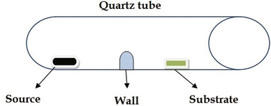 | Fig. 1 Schematic of the setup used for the growth of the ZnO nanowires |
The electric furnace was naturally cooled down to the room temperature. The crystal structure and morphology of the samples were investigated using a field emission scanning electron microscopy (FESEM, JSM 6700) and X-ray diffraction (XRD, Shimadzu 6000) employing CuKα (0.154 nm) radiation. The optical properties of the samples were characterized using a laboratory setup with a pulsed xenon lamp (LS-55, Xe lamp) and Raman (Jobin-Yvon Horiba HR 800 UV) spectroscopy.
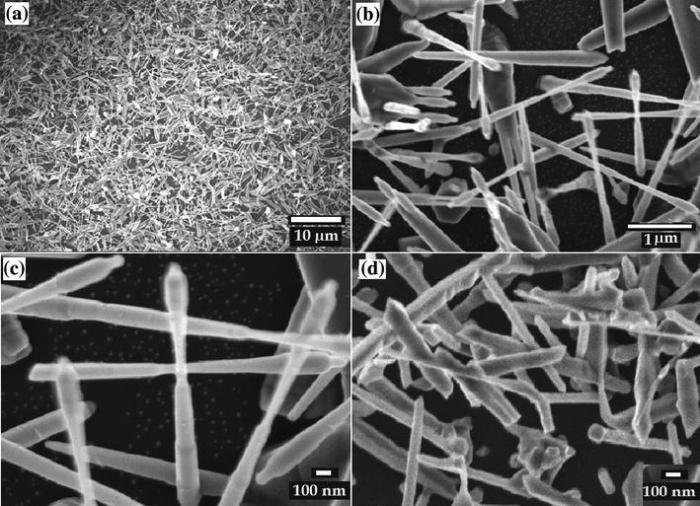
One sample (sample S1) was grown by the modified tube and a reference sample by the normal tube (sample S2). The morphology of the as-grown samples was examined using an FESEM. Figure 2a shows a low magnification FESEM image of sample S1. It can be seen that the pencil-like nanowires are grown in a very high density. The high magnification SEM images (Fig. 2b, c) indicate that each pencil consists of a pen-nib and holder. The diameters of the pen holders and pen-nibs are about 150 ± 50 and 50 ± 10 nm, respectively. The pencils have the lengths of about several microns.
 | Fig. 2 Typical FESEM images of the ZnO nanopencil grown in the modified tube a-c and ZnO nanostructure grown in the normal tube d |
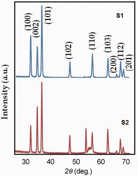
Figure 2d shows another typical morphology of ZnO nanostructure grown in the normal tube with no aluminum wall (sample S2). Versatile morphologies including nail, spear and rod nanostructures can be seen clearly. They have a range from 100 to 250 nm in diameter and several microns in length. The results demonstrate that the shapes of the products depend on the growth conditions. Placement of the wall between the source and the substrate may result in significantly lower vapor pressure of the reactants and thus better ordering and uniform shape of the nanostructures. To investigate the crystal structure of the samples, the XRD pattern of the pencil-like ZnO was examined. It was confirmed that the crystalline phase of the sample is the wurtzite structure (hexagonal with space group P63mc).
All diffraction peaks were indexed as shown in Fig. 3 and were in agreement with JCPDS 36-1451. The cell constants of a (0.325 nm) and c (0.521 nm) are quite similar to those of pure ZnO. No peaks from Zn or other impurities were detected.
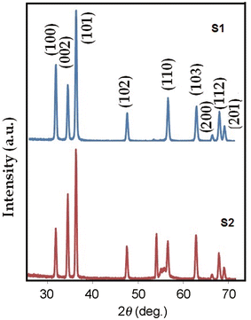 | Fig. 3 XRD patterns of the ZnO nanowires grown by modified (sample S1) and normal (sample S2) vapor method(1) |
The (002) peak was chosen to estimate the crystallite size D from the maximum intensity of the full width at half maximum (FWHM, β ) related to the films with different thicknesses. To calculate the crystallite size D, we used Debye-Scherrer’ s formula:
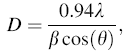 |
where λ is X-ray wavelength (0.15405 nm in this case), β is the diffraction line broadening at FWHM of the peak, and θ is the peak position. The results are presented in Table 1.
| Table 1 Comparison of position, height, FWHM, and crystallite size of (002) diffraction peaks |
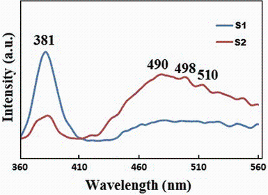
Studies of the luminescence of ZnO crystals indicate that two emission bands can be observed in the photoluminescence spectra: One is in the ultraviolet (UV) region around 380 nm or 3.25 eV, and the other a broad green band between 500 and 530 nm or 2.35-2.50 eV. It is generally accepted that the UV emission of ZnO can be attributed to the mixture of free exciton and other impurity-related transitions at the near-band edge (NBE) [10]. The band structure calculations propose that the deep-level green band emission (DLE) is attributed to singly ionized oxygen vacancy in ZnO. It came from recombination of a photogenerated hole with the singly ionized charge state of this defect [11]. The room temperature photoluminescence spectra of the products are shown in Fig. 4. The strong UV peaks (also called the near-band-edge (NBE) emission) at 381 nm with a narrow FWHM of 21 nm for sample S1 and a weaker one at 384 nm for sample S2 are observed in the spectra. The differences in the intensity and position of the UV peaks are due to the different growth conditions, the effect on the relative contributions of free exiton emission and phonon. In the case of the structure of nanopencils, the wall in the modified tube decreases the boundary layer thickness and causes the reduction in strain defects as well as improves the crystallize size.
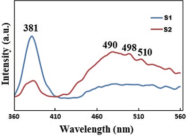 | Fig. 4 Room-temperature photoluminescence spectra, the ZnO nanopencil grown in the modified tube (sample S1), and the ZnO nanostructure grown in the normal tube (sample S2) |
For both samples S1 and S2, a dominant visible emission manifested as a broad feature in the range of 450-550 nm. Although the exact origin of this broad visible band emission is still an open question, it is suggested that it corresponds to the singly ionized oxygen vacancy in ZnO, the fast reaction formation process and the large surface-to-volume ratio [12, 13]. The ratio of the UV and visible intensity (UV/DLE) provides some indication of the material quality and comparison of optical properties between samples [14]. The high UV/DLE ratio of sample S1 compared with that of sample S2, in addition to the narrow UV peak and the decrease in the peak intensity of the green emission, could be the result of high crystalline quality of the pencils. In addition, the DLE is enhanced while the UV emission is suppressed due to the increase in both the oxygen vacancies and zinc interstitials of sample S2.
Raman scattering spectroscopy is a technique used to observe low-frequency modes such as rotation and vibration in a system. When a laser light interacts with molecular vibrations or phonons, the frequency of photons is shifted up or down. The change in the photon frequency provides information about molecular vibrations that can be used for structural defection and crystal perfection of the system.
Based on the vibrational modes, the thermal and electrical properties of a single crystal, such as the wurtzite ZnO structure, can be investigated.
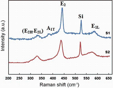
Figure 5 shows the characteristic Raman spectra features of both samples S1 and S2. Several bands related to Raman-active phonon modes of wurtzite ZnO nanostructure with C6 V symmetry can be observed. The strong Si peak is coming from the substrate.
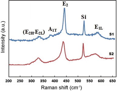 | Fig. 5 Raman spectra excited by 514-nm line, the ZnO nanopencil grown in the modified tube (sample S1), and the ZnO nanostructure grown in the normal tube (sample S2) |
The E2 (high) phonon frequency at 437 cm-1 is the intrinsic characteristic of hexagonal wurtzite ZnO [15]. The FWHM of the E2 (high) mode decreased from sample S2 to S1. Therefore, this result and the PL results indicate that the crystallinity of the nanopencils is higher than that of the nanowires in sample S2.
The E2 (high) mode of the wurtzite ZnO crystal structure would shift to a lower frequency under internal strains resulting in different growth conditions. The E2 (high) mode has been blueshifted (434 cm-1) for sample S2 compared with bulk ZnO (437 cm-1). Using the below equation [16], the stress value of sample S2 is found to be 0.454 (GPa).
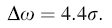 |
where σ is the stress of nanostructures in the c-axis direction in GPa and △w is the shift of E2 (high) mode in cm-1.
The forbidden mode attributed to the E2 (high)-E1 (low), or multi-phonon process mode is located at 331 cm-1 frequency of second order. This mode can only be found when the ZnO is a single crystal [17].
The peaks at 580 cm-1 corresponding to the E1 (LO) vibration mode are related to impurities and formation of defects such as oxygen vacancies, zinc interstitial and free carriers [18]. It seems that the E1 (LO) mode is broad and is enhanced by disorder [19].
The reason of the low intensity of them is due to more ordered wurtzite structures as seen in the peak at 438 cm-1. Additionally, Fig. 5 shows a peak at 380 cm-1 corresponding the A1 (TO) mode. This peak usually originated from structure or doping induced by disorder in the ZnO substrate.
As known, one-dimensional diffusion of a gas is written by Fick’ s first law:
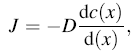 |
where J is the diffusion flux (amount of substance per unit area per unit time), D is the intrinsic diffusion coefficient, and c is the concentration at x.
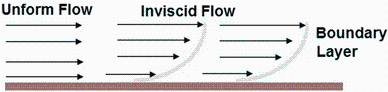
In the vapor phase transport (VPT) method, gaseous species move from the source region to the substrates through a layer of reduced velocity vapor, called boundary layer (Fig. 6). Under certain conditions adjacent to the wall, separation of the boundary layer can occur due to excessive momentum loss near the wall. In this condition, the gaseous species try to move downstream against increasing pressure which is called adverse pressure gradient. Somewhere around the top of the wall, the fluid particles in the boundary layer are separated from the wall and are driven in the upstream direction. The influence of the boundary layer separation on the surface reaction and adsorption, results in the overall growth rate and different morphologies [20].
 | Fig. 6 Illustration of a separation of boundary layer |
To explain the growth mechanism of the obtained nanostructure (pencil-like), the idealized growth habit of the ZnO crystal can be used. Vapor-solid (VS) growth process is suggested for the formation of this kind of crystal [21, 22].
The reactions that govern VPT growth of ZnO nanostructures are as follows:
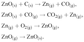
The melting point of solid ZnO is reduced (from 1975 to 910 ° C) by graphite. The gases produced by the first reaction are Zn (g) and CO (g). The Zn vapors transfer from high-temperature zones into the low-temperature zones and deposit on the substrate. The facet with higher surface energy is usually small in area, while the lower energy facets are larger. In zinc oxide nanostructures, the (0001) planes possess the highest surface energy among the low index planes. As a result, ZnO grows along the c-axis to minimize the surface area of the (0001) planes. The velocity of the crystal growth is related to the different directions as: 
The formation of pen holder part with high aspect ratio is attributed to the [0001] direction with the fastest growth rate [24]. In a general growth habit of crystal, crystal face whose growth rate is fast disappears easily, while faces whose growth rates are slow remain. Thus, 

A novel pencil-like ZnO nanowire has been grown on the Si (111) substrate via a modified vapor phase transport method under air atmosphere. A wall (aluminum foil) of 1 cm in height was inserted between the source and substrate to study the effect of the wall on the morphological and optical properties of the samples. It was found that a separation of the boundary layer on the top of the wall disturbed Zn diffusion and affected the diameter of the wires. Thus, difference in the diameters of the wires provided pencil-like shape. The obtained Pl and Raman spectra verify that the optical properties of ZnO nanostructures grown under different growth conditions are very sensitive to preparation conditions and morphology.
This work was supported by the Universiti Putra Malaysia through Grant Nos. Fundamental Research Grant Scheme (FRGS) vote: 02-01-14-1469FR.
The authors have declared that no competing interests exist.
| [1] |
|
| [2] |
|
| [3] |
|
| [4] |
|
| [5] |
|
| [6] |
|
| [7] |
|
| [8] |
|
| [9] |
|
| [10] |
|
| [11] |
|
| [12] |
|
| [13] |
|
| [14] |
|
| [15] |
|
| [16] |
|
| [17] |
|
| [18] |
|
| [19] |
|
| [20] |
|
| [21] |
|
| [22] |
|
| [23] |
|
| [24] |
|