V. Chandrakala, J. Annai Joseph Steffy, Neena Bachan, W. Jothi Jeyarani, Tenzin Tenkyong, J. Merline Shyla1. A Comparative Investigation of Dye-Sensitized Titanium Dioxide (TiO2) Nanorods Grown on Indium Tin Oxide (ITO) Substrates by Direct and Seed-Mediated Hydrothermal Methods . Acta Metallurgica Sinica(English Letters), 2016, 29(5): 457
Copyright reserved, Editorial board of Acta Metallurgica Sinica(English Letters)
A Comparative Investigation of Dye-Sensitized Titanium Dioxide (TiO2) Nanorods Grown on Indium Tin Oxide (ITO) Substrates by Direct and Seed-Mediated Hydrothermal Methods
V. Chandrakala, J. Annai Joseph Steffy, Neena Bachan, W. Jothi Jeyarani, Tenzin Tenkyong, J. Merline Shyla1
Department of Physics, Energy Nanotechnology Centre (ENTeC), Loyola Institute of Frontier Energy (LIFE), Loyola College, Chennai 600 034, India
We report a comparative investigation of the characteristics of modified TiO2 nanorods grown on conducting indium tin oxide glass (ITO) substrates by two different hydrothermal methods: the direct method by which rutile TiO2 nanorods were grown directly on plain ITO substrates and the seed-mediated one using which a thin film of anatase TiO2 seed layer was laid down by spin coating and annealing prior to the growth of TiO2 nanorods on it. Microstructural analysis of the samples using X-ray diffraction confirmed their rutile nature. The average crystallite size estimated using Scherrer’s formula was found to fall in the range of 11-17 nm in both cases. Field emission scanning electron microscopy revealed the nanorod morphologies of a dandelion arrangement in the case of directly grown ones and a proper vertical orientation in the case of the seed-mediated method. UV-Vis spectroscopy analysis of both the samples exhibited redshifts with intense absorption of visible radiation, and the seed-mediated one was found to possess an increased bandgap. The transport nature of the samples was characterized by significant increase in both dark and photocurrents. The results show that the dark and photocurrent values of the directly grown TiO2 nanorods were greater than those of the seed-mediated ones by ~seven and five folds, respectively, and therefore, it could serve as efficient photoelectrodes in dye-sensitized solar cells.
Keyword:
Dye-sensitized solar cells; Hydrothermal; Seed-mediated; Photoconductivity; Spin coating; Safranine O dye; TiO2 nanorods
Dye-sensitized solar cells (DSSCs) [1], a promising alternative to the conventional silicon-based solar cells [2], have been introduced to utilize solar energy using porous nanocrystalline Titania (TiO2) film in conjunction with an efficient light-absorbing dye [3, 4]. TiO2 has been a material of interest in various applications due to its excellent physical and chemical stability together with the oxidizing ability of its photogenerated holes[5, 6]. A power conversion efficiency of 12.3% has been reported for TiO2 mesoporous film owing to the high surface area [7]. Nevertheless, the interconnected nanoparticle grain boundaries result in reduced electron transport rate [8, 9].
Recently, one-dimensional (1D) TiO2 nanostructures, such as nanotubes [10], nanorods[11]and nanowires [12], have gained much importance in solar energy research as they serve as platforms conducive for electron transport, reported to be of several orders of magnitude higher than that of plain TiO2 nanoparticles [13, 14]. Among such one-dimensional nanostructures, TiO2 nanorods have found extensive applications in devices such as DSSCs [15], gas sensors [16] and lithium batteries [17] due to their distinctive optical, electrical and catalyst properties [18] which yield fast charge transport of photogenerated carriers along a longitudinal direction, reduced rate of recombination and effective light scattering ability within the nanostructure [19, 20]. Due to their unique characteristics and higher photoelectrochemical conversion in DSSCs and in order to present them as enhanced potential photoelectrodes, the synthesis and study of 1D TiO2 nanorods were undertaken in the present work. One-dimensional TiO2 nanostructures are generally synthesized by wet chemical routes such as hydrothermal[21, 22], solvothermal[23, 24], sol-gel template [25, 26], sonochemical synthesis [27] and sputtering techniques [28]. Among these, hydrothermal synthesis is a promising approach due to its simple process, fast reaction velocity and low cost. It also provides an effective reaction environment that gives control of the size, morphology and crystal modification of the product [29]. Therefore, in the present work, the hydrothermal method has been preferred for the preparation of TiO2 nanorod thin films.
Previous reports had suggested that TiO2 nanorods could be grown only on FTO substrates [30]. However, subsequent investigations revealed that they could be fabricated on varied substrates by coating them with a preceding seed layer and carefully controlling the vital parameters affecting growth [31]. In the present study, we report a seed-mediated fabrication technique to grow rutile TiO2 nanorods hydrothermally over a seed layer of spin-coated anatase TiO2 thin film deposited prior on indium tin oxide substrate. To carry out a comparative investigation and also to study the significance of the seed mediation, TiO2 nanorods were also grown directly on ITO substrate without the seed layer. Both the samples were then dye-sensitized with Safranine O dye to examine their suitability for use as photoelectrodes in DSSCs. This kind of pilot testing of a dye-sensitized photoelectrode to examine its pertinence as a potential photoelectrode even before the construction of the DSSC is a less investigated work and is expected to provide significant insights into its possible yield when employed as a working electrode.
2 Experimental
2.1 Synthesis
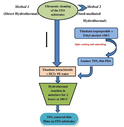
Titanium isopropoxide (C12H28O4Ti), titanium tetrachloride (TiCl4), hydrochloric acid (37 wt% HCl) and ethyl alcohol (C2H6O) were purchased from Fisher Scientific and used as received. The ITO substrates (40 Ω cm-2) of desired sizes (2 cm × 2 cm) were taken and ultrasonically cleaned with acetone and distilled water in sequence for 10 min. In a typical experiment, 1 mL of titanium isopropoxide dissolved in a mixture containing 10 mL of ethyl alcohol and 0.25 mL of hydrochloric acid was spin-coated on the selected substrate at a spinning speed of 3000 r/min and dried at 60 ° C for 6 h. The coated substrate was then annealed in a furnace at 600 ° C for 1 h in order to make it crystalline[32]. For the hydrothermal synthesis, 20 mL of HCl was mixed with 25 mL of deionized water and stirred at an ambient temperature for 5 min and 0.2 mL of TiCl4 was subsequently added to the above solution. The as-prepared solution was poured into a Teflon-lined stainless steel autoclave and the plain or spin-coated ITO substrate was placed at an angle with the conducting side facing downwards and heated at 180 ° C for 2 h in a furnace. The autoclave was then cooled to room temperature, and the substrate was washed with deionized water and dried in air[33]. By the procedure described above, two samples were prepared— one by the direct hydrothermal method and the other by seed-mediated hydrothermal method (i.e., ITO substrate was spin-coated with seed layer prior to the hydrothermal treatment), and a comparative analysis was performed. Schematic representation of the synthesis procedure is given in Fig. 1.
The TiO2 nanorod films were then immersed into Safranine O dye solution (0.3 mmol in 10 mL ethanol) and stored at room temperature for 24 h, which resulted in an intense coloration of the film surface [34].
Fig. 1 Schematic representation of the synthesis procedure of TiO2 nanorods on ITO substrates
2.2 Characterization
The crystal structure of the TiO2 nanorod thin films was studied by Rigaku X-ray diffractometer (XRD, Japan) employing CuK α at 9 kW. The diffraction patterns were recorded over the 2θ range 20° -80° by scanning with a step size of 0.02° . The morphologies and size distribution of the synthesized samples were investigated using FESEM (SUPRA-55, Carl Zeiss, Germany). The UV-Vis absorption spectra were obtained using UV-Vis-Cary 5 spectrophotometer (Santa Clara, USA). The spectra were recorded at room temperature in the range 200-800 nm. Field-dependent dark and photoconductivity studies were carried out using Keithley 6485 picoammeter (Ohio, USA). The experimental setup for the measurement of field-dependent dark and photoconductivity is as used by Ponniah and Xavier [35]. In the thin-film samples, two electrodes of thin copper wire were fixed using silver paint. The ends of the copper wire were connected to a DC power supply through the picoammeter. The applied field was varied and the corresponding current in the circuit was measured. To record the photocurrent, light from a 100-W halogen lamp was illuminated over the sample and the same procedure elaborated above was followed.
3 Results and Discussion
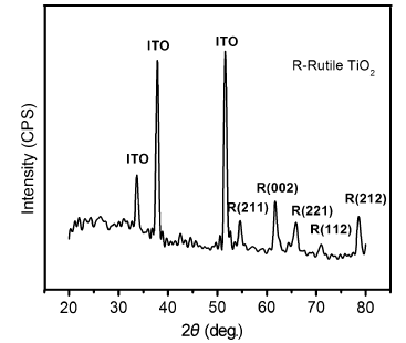
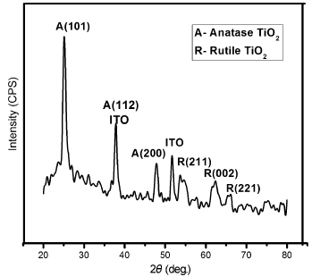
The X-ray diffraction patterns of the samples grown by direct and seed-mediated hydrothermal methods are shown in Figs. 2 and 3, respectively. From the XRD pattern of the hydrothermally grown TiO2 nanorods, it is evident that the TiO2 nanorods grown on ITO-coated glass substrates have a tetragonal rutile structure. The diffraction peaks at 2θ = 54.7° , 61.5° , 65.9° , 72.9° and 78.6° correspond to the (211), (002), (221), (112) and (212) planes of rutile TiO2 (JCPDS card no. 21-1276), whereas those at 34° , 38° and 51° are from the ITO substrate (JCPDS card no. 88-0773). The sharp diffraction peaks indicate that the sample is well crystallized and the results were found to be in excellent agreement with similar reported work[33].
Fig. 3 XRD pattern of TiO2 nanorods grown on ITO-glass substrates by seed-mediated hydrothermal method
The diffraction peaks in the XRD pattern of seed-mediated hydrothermally grown TiO2 nanorods revealed the presence of both anatase and rutile phases. This polycrystalline nature was due to the possibility that the spin-coated seed layer which possessed pronounced anatase peaks could have gradually given rise to rutile peaks upon hydrothermal treatment, thereby indicating a phase transformation from anatase nanoparticles to rutile nanostructures [36]. The peak positions at 2θ = 25.2° , 38° and 48° correspond to the anatase phases of (101), (112) and (200) orientations (JCPDS card no. 89-4920). The peak at 38° could additionally correspond to the ITO substrate. The diffraction peaks at 2θ = 54.4° , 62.8° and 65.6° correspond to rutile planes of (211), (002) and (221) orientations. The XRD pattern further indicates that the (101) plane could be the side wall of TiO2 nanorod structures which is preferentially exposed to the X-rays. The results were in good agreement with similar reported work[37].
The average crystallite sizes of both samples were calculated by the Scherrer’ s equation: D = 0.89λ /(β cosθ ), where λ is the X-ray wavelength, θ is the Bragg angle and β is the line broadening at half the maximum intensity (FWHM) [38]. The average crystallite sizes thus obtained in the case of seed-mediated TiO2 nanorods were 10.7 and 11.68 nm in the (101) and (112) planes, respectively, for the anatase phase and ranged from 11 to 17 nm for the rutile phase. The crystallite size was found to be dependent on annealing temperature and increased upon phase transformation from anatase to rutile. The average crystallite size estimated in the case of directly grown TiO2 nanorods was also found to be in the range between 11 and 17 nm. The results from both the methods indicated that the average crystallite size of (211) plane was higher than the other planes, suggesting that the longitudinal direction of the nanorod would bind within the (211) plane in order to minimize the total surface energy for attaining thermodynamic equilibrium [30, 37].
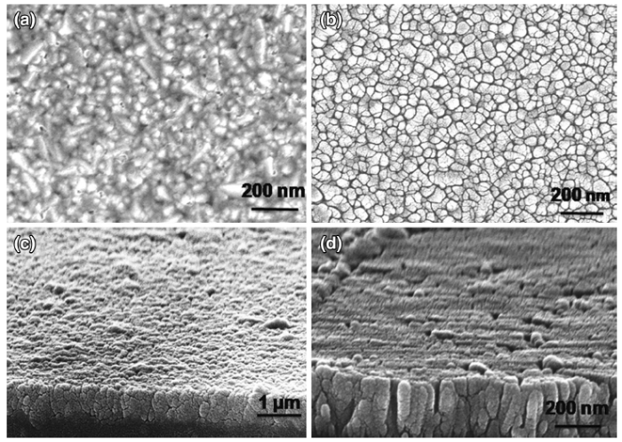
Figure 4 shows the FESEM images of TiO2 nanorods on ITO substrate by direct and seed-mediated hydrothermal methods using TiCl4 as the precursor. From the FESEM images of direct hydrothermal method, it was evident that the formation of dandelion-type nanostructures which is desirable in the case of nanorods was not very significantly observed. However, dandelions of comparatively lower density and smaller size were visible. The length of the nanorods measured from FESEM investigations was found to be of approximately 447 nm concurring with earlier reports[36].
Fig. 4 Top a and cross-sectional c views of the TiO2 nanorods grown by direct hydrothermal method; top b and cross-sectional d views of the TiO2 nanorods grown by seed-mediated hydrothermal method
In the case of seed-mediated hydrothermally grown TiO2 nanorods, a preferred vertical orientation was apparent. The lattice mismatch between the substrate and the TiO2 nanorods was avoided by the seed-mediation process which facilitated the growth of well-defined nanorods with preferred orientation and dandelion-like morphology due to the presence of spin-coated seed layer[5].
FESEM images also indicate that the TiO2 nanorod arrays were well ordered and aligned. Nearly uniform growth was further evident over the entire substrate though with traces of agglomeration. Agglomeration was apparently due to the high surface energy of nanoparticles which exhibit a tendency to stabilize themselves as spherical agglomerates in order to possess the minimum surface to volume ratio which essentially leads to a decreased active surface area available for dye absorption and a consequent fall in the photocurrent [39]. Agglomeration in the photoelectrode generally reduces the area of interconnection between the nanoparticles by decreasing their electrical contact, thereby increasing the resistance for charge transfer. This would lead to an upsurge in electron recombination by the suppression of electron flow in DSSC, thus decreasing its efficiency [40]. The present work suggests that the fabrication of TiO2 nanorods on ITO substrate could be well accomplished by the direct hydrothermal method even in the absence of an epitaxial interface. Nevertheless, a seed layer that ensures an epitaxial interface between the TiO2 layer and the substrate is a prerequisite for the synthesis of highly aligned and well-oriented nanorod arrays [5].
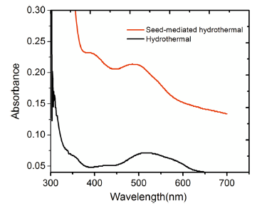
The safranine O dye-sensitized titania nanorod array samples were analyzed with UV-Visible absorption spectrophotometry, and the spectra are as shown in Fig. 5. The intensity of the dye absorption peaks of the two samples varied widely with the absorption edges redshifting at 525 nm (close to the bandgap of safranine O dye (2.37 eV)) in the visible region of the spectrum in both cases. The above result is a distinctive aspect of charge transfer transitions occurring due to the electron transfer between dye and TiO2 molecules [41]. It could be seen that the seed-mediated hydrothermal sample exhibits the highest absorption peak with a broader and higher range of absorption, but it is blueshifted in comparison with that of the direct hydrothermal method. The absorption intensity could be enhanced with the increase in dye quantity on TiO2 nanorods, and hence, the absorption edge is expected to gradually move toward a longer wavelength (redshift) in the entire UV-Visible region [42].
Fig. 5 Optical absorption spectra of Safranine O dye-sensitized TiO2 nanorods grown on ITO substrate by seed-mediated and direct hydrothermal methods
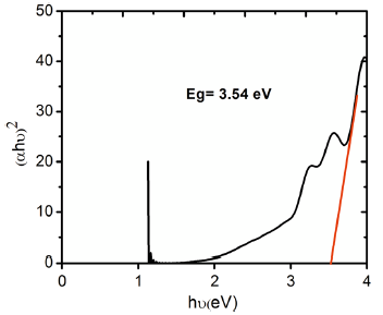
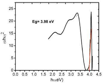
From the UV-Visible absorption spectra (Fig. 5), the optical bandgap energy E g of the safranine O dye-sensitized TiO2 nanorods was estimated by employing Tauc’ s method. An extrapolation of the decreasing slope to zero of the plot between (α hν )2 and hν in Figs. 6 and 7 yielded the optical energy gap values, where α is the absorption coefficient and hν the photon energy[43].
Fig. 7 Tauc’ s plot of Safranine O dye-sensitized TiO2 nanorods grown on ITO-glass substrates by seed-mediated hydrothermal method
From the plots, the bandgap values of safranine O dye-sensitized TiO2 nanorods were estimated as 3.54 and 3.98 eV for direct and seed-mediated hydrothermally grown samples, respectively. The bandgap energies (E g) of as-prepared TiO2 nanorods by both the methods were found to be larger than that of bulk TiO2 (3.2 eV), and it could be explained with the dependence of the bandgap of semiconductors on particle size which tends to increase with decreasing particle size[44].
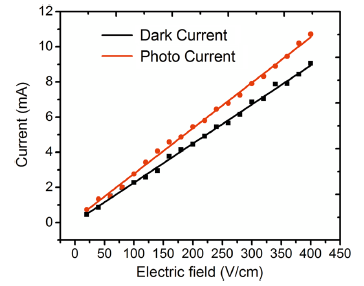
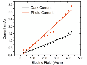
The variation in dark and photocurrent values with applied field for the safranine O dye-sensitized samples was plotted and is shown in Figs. 8 and 9, respectively. It was observed that the plots in both cases were linear illustrating the ohmic behavior of the samples[45].
Fig. 8 The field-dependent dark and photoconductivity of Safranine O dye-sensitized TiO2 nanorod arrays fabricated on the ITO substrates by direct hydrothermal method
Fig. 9 The field-dependent dark and photoconductivity of Safranine O dye-sensitized TiO2 nanorod arrays fabricated on the ITO substrates by seed-mediated hydrothermal method
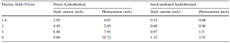
In general, the dark and photocurrent values of the dye-sensitized TiO2 nanorods were found to record a significant increase as compared to pure TiO2 nanoparticles as the range is in milliampere in contrast to microampere in the case of the latter [46]. Further, photocurrent in respect of both samples was found to be higher than the dark current, indicating that the dye-sensitized nanostructures are photoconducting in nature due to enhanced coupling of TiO2 nanorods with safranine O dye molecules on the surface which increases the electron injection by improved light absorption in the visible region [41]. In the case of TiO2 nanorods grown by direct hydrothermal method, for a fixed applied electric field of 1.4 V/cm, the photocurrent was found to be about 1.4 times higher than the corresponding dark current. For the seed-mediated hydrothermally grown nanorods also, the photocurrent was observed to be about 1.3 times higher than the dark current and the comparative data are presented in Table 1.
Table 1
Table 1
Table 1 Comparative field-dependent dark and photoconductivity values
Table 1 Comparative field-dependent dark and photoconductivity values
On comparison of the two samples for a fixed field of 3 V/cm, the dark and photocurrent values of the directly grown sample were found to be greater than that of the seed-mediated ones by about ~seven- and fivefold, respectively. The significant increase in dark and photocurrent values in the case of directly grown nanorods in comparison with the seed-mediated hydrothermally grown samples could be attributed to the observation that in the case of the former, the surface was found to be filled with nanorods (though not oriented in a particular direction) which effectively promote the transport of charge on the surface[47]. However, in the case of the latter though a preferred orientation was observed it was accompanied by agglomeration and cluster formation which could have hindered the conductivity on the surface[48]. Nevertheless, better absorption of the dye in the case of seed-mediated hydrothermally grown nanorods could yield higher photocurrents when used as electrodes in DSSCs, provided that the sample texture is improved by preventing cluster formation and agglomeration. Thus, it could be concluded that the surface conductivity of the hydrothermally grown TiO2 nanorods is enhanced considerably owing to its surface morphology and homogeneity[49, 50].
4 Conclusions
This paper has presented a comparative investigation of the characteristics of TiO2 nanorods synthesized on ITO substrates by direct and seed-mediated hydrothermal methods. Rutile TiO2 nanorods in the form of small dandelions were observed in the direct hydrothermal method, whereas vertically aligned TiO2 nanorods were seen in the case of seed-mediated method. The UV-Vis analysis of the dye-sensitized TiO2 nanorods, in both cases, revealed redshifts with intense absorption of visible radiation in comparison with TiO2 nanoparticles, owing to the enhanced charge transfer process between the dye and TiO2 molecules facilitated by the rod morphology. Upon dye sensitization, both samples show excellent photoconductive behavior when compared to pure TiO2 nanoparticles with the directly grown ones recording a higher yield of surface conductivity. As an outlook, this research paper would like to accentuate that one-dimensional TiO2 nanorods grown on ITO substrate by the direct hydrothermal method (without seed layer) could serve as efficient photoelectrodes in DSSCs.
Acknowledgments
This work has been partially funded by the Loyola College-Times of India Major Research Grants (6LCTOI14LIF002) and the authors acknowledge the same.
The authors have declared that no competing interests exist.
P. Soundarrajan, K. Sankarasubramanian, T. Logu, K. Sethuraman, K. Ramamurthi, Mater. Lett. 116, 191(2014)[Cite with in:1]
[12]
Y. Wang, H. Yang, H. Xu, Mater. Lett. 64, 164(2010)[Cite with in:1]
[13]
K. H. Yu, J. H. Chen, Nanoscale Res. Lett. 4, 1(2010)[Cite with in:1]
[14]
T. Yuan, H. B. Lu, B. H. Dong, L. Zhao, L. Wan, S. M. Wang, Z. X. Xu, J. Mater. Sci. Mater. Electron. 36, 1332(2014)[Cite with in:1]
[15]
J. J. Zhu, Y. L. Zhao, L. Zhu, X. Q. Gu, Y. H. Qiang, Chin. Phys. B23, 048104 (2014)[Cite with in:1]
[16]
W. C. Tian, Y. H. Ho, C. H. Chen, C. Y. Kuo, Sensors13, 865(2013)[Cite with in:1]
[17]
H. Qiao, Q. Luo, Q. Wei, Y. Cai, F. Huang, Ionics18, 667(2012)[Cite with in:1]
[18]
Q. Zhang, G. Chen, Y. Yang, X. Shen, Y. Zhang, C. Li, R. Yu, Y. Luo, D. Li, Q. Meng, Phys. Chem. Chem. Phys. 14, 6479(2012)[Cite with in:1]
[19]
J. Liang, G. M. Zhang, J. Yang, W. T. Sun, M. J. Shi, AIP Adv. 5, 017141(2015)[Cite with in:1]
[20]
Q. L. Huang, G. Zhou, L. Fang, L. P. Hu, Z. Wang, Energy Environ. Sci. 4, 2145 (2011)[Cite with in:1]
[21]
S. J. Kwon, H. B. Im, J. E. Nam, J. K. Kang, T. S. Hwang, K. B. Yi, Appl. Surf. Sci. 320, 487(2014)[Cite with in:1]
[22]
P. Soundarrajan, K. Sankarasubramanian, K. Sethuraman, K. Ramamurthi, Controlled (110and (101) crystallographic plane growth of single crystalline rutile TiO2 nanorods by facile low cost chemical methods. Cryst. Eng. Commun. 16, 8756(2014)[Cite with in:1]
[23]
S. Kim, M. S. Kim, H. Park, G. Nam, H. Yoon, J. Y. Leem, Electron. Mater. Lett. 10, 565(2014)[Cite with in:1]
[24]
J. Liu, J. Luo, W. G. Yang, Y. L. Wang, L. Y. Zhu, Y. Y. Xu, Y. J. Hu, C. Wang, Y. G. Chen, W. M. Shi, Y. Tang, J. Mater. Sci. Technol. 31, 106(2015)[Cite with in:1]
[25]
M. Riazian, Indian J. Chem. Sec A51, 1377 (2014)[Cite with in:1]
[26]
M. A. Mohamed, J. Jaafar, W. N. W. J. Sol-Gel. Sci. Technol. 74, 513(2015)[Cite with in:1]
[27]
H. Arami, M. Mazloumi, R. Khalifehzadeh, S. K. Sadrnezhaad, Mater. Lett. 61, 4559(2007)[Cite with in:1]
[28]
L. J. Meng, H. Chen, C. Li, Thin Solid Films577, 103 (2015)[Cite with in:1]
[29]
Z. Wei, Y. Yao, T. Huang, A. S. Yu, Int. J. Electrochem. Sci. 6, 1871(2011)[Cite with in:1]
H. E. Wang, Z. Chen, Y. H. Leung, C. Luan, C. Liu, Y. Tang, C. Yan, W. J. Zhang, J. A. Zapien, I. Bello, S. T. Lee, Appl. Phys. Lett. 96, 263104(2010)[Cite with in:1]
[32]
U. Ullaspradhan, S. K. Arch. Phys. Res. 4, 121(2011)[Cite with in:1]
[33]
Y. T. Li, L. Wei, R. Z. Zhang, Y. X. Chen, L. M. Mei, J. Jiao, Nanoscale Res. Lett. 8, 89(2013)[Cite with in:2]
[34]
I. Su-Il, P. Klaus, H. Lee, H. Inge, D. D. Qin, N. Z. Bao, C. A. Grimes, Bull. Korean Chem. Soc. , 331981 (2012)[Cite with in:1]
[35]
D. Ponniah, F. Xavier, Phys. B392, 20 (2007)[Cite with in:1]
[36]
J. G. Wua, S. Lo, K. Song, B. K. Vijayan, W. Y. Li, K. A. Gray, V. P. Dravid, J. Mater. Res. 26, 1646(2011)[Cite with in:2]
[37]
S. Navaladian, B. Viswanathan, T. K. Varadarajan, R. P. Viswanath, Nanoscale Res. Lett. 4, 471(2009)[Cite with in:2]
M. Sakar, S. Balakumar, P. Saravanan, S. N. Jaisankar, Mater. Res. Bull. 48, 2878(2013)[Cite with in:1]
[40]
A. Sedghi, H. N. Miankushki, Int. J. Electrochem. Sci. 7, 12078(2012)[Cite with in:1]
[41]
D. Arunkumar, F. P. Xavier, J. M. Shyla, Arch. Appl. Sci. Res. 4, 2122 (2012)[Cite with in:2]
[42]
L. J. Guo, D. W. Jing, M. C. Liu, Y. B. Chen, S. H. Shen, J. W. Shi, K. Zhang, Beilstein J. Nanotechnol. 5, 994(2014)[Cite with in:1]
[43]
N. Bachan, A. Asha, W. JothiJeyarani, D. Kumar, J. Shyla, ActaMetall. Sin. (Engl. Lett. ) 28, 1317(2015)[Cite with in:1]
[44]
R. Danish, F. Ahmed, N. Arshi, M. S. Anwar, B. H. Koo, Trans. Nonferrous Met. Soc. China24, s152 (2014)[Cite with in:1]
[45]
J. MerlineShyla, F. P. Xavier, P. Sagayaraj, Int. J. Microstruct. Mater. Prop. 8, 6(2013)[Cite with in:1]
[46]
D. Arunkumar, J. A. Xavier, J. M. Shyla, F. P. Xavier, J. Mater. Sci. 48, 3700(2013)[Cite with in:1]
[47]
A. E. Shalan, M. M. Rashad, Y. H. Yu, M. Lira-Cantu´, M. S. A. Appl. Phys. A110, 111 (2013)[Cite with in:1]
[48]
B. Koo, J. Park, Y. Kim, S. H. Choi, Y. E. Sung, T. Hyeon, J. Phys. Chem. B110, 24318 (2006)[Cite with in:1]
[49]
M. Adachi, Y. Murata, J. Takao, J. Jiu, M. Sakamato, F. Wang, J. Am. Chem. Soc. 126, 14943(2004)[Cite with in:1]
[50]
E. Karber, A. Katerski, I. O. Acik, M. Mere, I. Sildos, M. Krunks, Beilstein J. Nanotechnol. 5, 2398(2014)[Cite with in:1]
1
2001
0.0
0.0
... 1 IntroductionDye-sensitized solar cells (DSSCs) [1], a promising alternative to the conventional silicon-based solar cells [2], have been introduced to utilize solar energy using porous nanocrystalline Titania (TiO2) film in conjunction with an efficient light-absorbing dye [3, 4] ...
1
2013
0.0
0.0
... 1 IntroductionDye-sensitized solar cells (DSSCs) [1], a promising alternative to the conventional silicon-based solar cells [2], have been introduced to utilize solar energy using porous nanocrystalline Titania (TiO2) film in conjunction with an efficient light-absorbing dye [3, 4] ...
1
2014
0.0
0.0
... 1 IntroductionDye-sensitized solar cells (DSSCs) [1], a promising alternative to the conventional silicon-based solar cells [2], have been introduced to utilize solar energy using porous nanocrystalline Titania (TiO2) film in conjunction with an efficient light-absorbing dye [3, 4] ...
1
2015
0.0
0.0
... 1 IntroductionDye-sensitized solar cells (DSSCs) [1], a promising alternative to the conventional silicon-based solar cells [2], have been introduced to utilize solar energy using porous nanocrystalline Titania (TiO2) film in conjunction with an efficient light-absorbing dye [3, 4] ...
3
2010
0.0
0.0
... TiO2 has been a material of interest in various applications due to its excellent physical and chemical stability together with the oxidizing ability of its photogenerated holes [5, 6] ...
... The lattice mismatch between the substrate and the TiO2 nanorods was avoided by the seed-mediation process which facilitated the growth of well-defined nanorods with preferred orientation and dandelion-like morphology due to the presence of spin-coated seed layer [5] ...
... Nevertheless, a seed layer that ensures an epitaxial interface between the TiO2 layer and the substrate is a prerequisite for the synthesis of highly aligned and well-oriented nanorod arrays [5] ...
1
2012
0.0
0.0
... TiO2 has been a material of interest in various applications due to its excellent physical and chemical stability together with the oxidizing ability of its photogenerated holes [5, 6] ...
1
2011
0.0
0.0
... 3% has been reported for TiO2 mesoporous film owing to the high surface area [7] ...
1
2013
0.0
0.0
... Nevertheless, the interconnected nanoparticle grain boundaries result in reduced electron transport rate [8, 9] ...
1
2014
0.0
0.0
... Nevertheless, the interconnected nanoparticle grain boundaries result in reduced electron transport rate [8, 9] ...
1
2015
0.0
0.0
... Recently, one-dimensional (1D) TiO2 nanostructures, such as nanotubes [10], nanorods [11] and nanowires [12], have gained much importance in solar energy research as they serve as platforms conducive for electron transport, reported to be of several orders of magnitude higher than that of plain TiO2 nanoparticles [13, 14] ...
1
2014
0.0
0.0
... Recently, one-dimensional (1D) TiO2 nanostructures, such as nanotubes [10], nanorods [11] and nanowires [12], have gained much importance in solar energy research as they serve as platforms conducive for electron transport, reported to be of several orders of magnitude higher than that of plain TiO2 nanoparticles [13, 14] ...
1
2010
0.0
0.0
... Recently, one-dimensional (1D) TiO2 nanostructures, such as nanotubes [10], nanorods [11] and nanowires [12], have gained much importance in solar energy research as they serve as platforms conducive for electron transport, reported to be of several orders of magnitude higher than that of plain TiO2 nanoparticles [13, 14] ...
1
2014
0.0
0.0
... Recently, one-dimensional (1D) TiO2 nanostructures, such as nanotubes [10], nanorods [11] and nanowires [12], have gained much importance in solar energy research as they serve as platforms conducive for electron transport, reported to be of several orders of magnitude higher than that of plain TiO2 nanoparticles [13, 14] ...
1
2014
0.0
0.0
... Among such one-dimensional nanostructures, TiO2 nanorods have found extensive applications in devices such as DSSCs [15], gas sensors [16] and lithium batteries [17] due to their distinctive optical, electrical and catalyst properties [18] which yield fast charge transport of photogenerated carriers along a longitudinal direction, reduced rate of recombination and effective light scattering ability within the nanostructure [19, 20] ...
1
2013
0.0
0.0
... Among such one-dimensional nanostructures, TiO2 nanorods have found extensive applications in devices such as DSSCs [15], gas sensors [16] and lithium batteries [17] due to their distinctive optical, electrical and catalyst properties [18] which yield fast charge transport of photogenerated carriers along a longitudinal direction, reduced rate of recombination and effective light scattering ability within the nanostructure [19, 20] ...
1
2012
0.0
0.0
... Among such one-dimensional nanostructures, TiO2 nanorods have found extensive applications in devices such as DSSCs [15], gas sensors [16] and lithium batteries [17] due to their distinctive optical, electrical and catalyst properties [18] which yield fast charge transport of photogenerated carriers along a longitudinal direction, reduced rate of recombination and effective light scattering ability within the nanostructure [19, 20] ...
1
2015
0.0
0.0
... Among such one-dimensional nanostructures, TiO2 nanorods have found extensive applications in devices such as DSSCs [15], gas sensors [16] and lithium batteries [17] due to their distinctive optical, electrical and catalyst properties [18] which yield fast charge transport of photogenerated carriers along a longitudinal direction, reduced rate of recombination and effective light scattering ability within the nanostructure [19, 20] ...
1
2145
0.0
0.0
... Among such one-dimensional nanostructures, TiO2 nanorods have found extensive applications in devices such as DSSCs [15], gas sensors [16] and lithium batteries [17] due to their distinctive optical, electrical and catalyst properties [18] which yield fast charge transport of photogenerated carriers along a longitudinal direction, reduced rate of recombination and effective light scattering ability within the nanostructure [19, 20] ...
1
2014
0.0
0.0
... One-dimensional TiO2 nanostructures are generally synthesized by wet chemical routes such as hydrothermal [21, 22], solvothermal [23, 24], sol-gel template [25, 26], sonochemical synthesis [27] and sputtering techniques [28] ...
1
2014
0.0
0.0
... One-dimensional TiO2 nanostructures are generally synthesized by wet chemical routes such as hydrothermal [21, 22], solvothermal [23, 24], sol-gel template [25, 26], sonochemical synthesis [27] and sputtering techniques [28] ...
1
2014
0.0
0.0
... One-dimensional TiO2 nanostructures are generally synthesized by wet chemical routes such as hydrothermal [21, 22], solvothermal [23, 24], sol-gel template [25, 26], sonochemical synthesis [27] and sputtering techniques [28] ...
1
2015
0.0
0.0
... One-dimensional TiO2 nanostructures are generally synthesized by wet chemical routes such as hydrothermal [21, 22], solvothermal [23, 24], sol-gel template [25, 26], sonochemical synthesis [27] and sputtering techniques [28] ...
1
2007
0.0
0.0
... One-dimensional TiO2 nanostructures are generally synthesized by wet chemical routes such as hydrothermal [21, 22], solvothermal [23, 24], sol-gel template [25, 26], sonochemical synthesis [27] and sputtering techniques [28] ...
1
2015
0.0
0.0
... One-dimensional TiO2 nanostructures are generally synthesized by wet chemical routes such as hydrothermal [21, 22], solvothermal [23, 24], sol-gel template [25, 26], sonochemical synthesis [27] and sputtering techniques [28] ...
1
2011
0.0
0.0
... It also provides an effective reaction environment that gives control of the size, morphology and crystal modification of the product [29] ...
2
2009
0.0
0.0
... Previous reports had suggested that TiO2 nanorods could be grown only on FTO substrates [30] ...
... The results from both the methods indicated that the average crystallite size of (211) plane was higher than the other planes, suggesting that the longitudinal direction of the nanorod would bind within the (211) plane in order to minimize the total surface energy for attaining thermodynamic equilibrium [30, 37] ...
1
2010
0.0
0.0
... However, subsequent investigations revealed that they could be fabricated on varied substrates by coating them with a preceding seed layer and carefully controlling the vital parameters affecting growth [31] ...
1
2011
0.0
0.0
... C for 1 h in order to make it crystalline [32] ...
2
2013
0.0
0.0
... The autoclave was then cooled to room temperature, and the substrate was washed with deionized water and dried in air [33] ...
... The sharp diffraction peaks indicate that the sample is well crystallized and the results were found to be in excellent agreement with similar reported work [33] ...
1
1981
0.0
0.0
... 3 mmol in 10 mL ethanol) and stored at room temperature for 24 h, which resulted in an intense coloration of the film surface [34] ...
1
2007
0.0
0.0
... The experimental setup for the measurement of field-dependent dark and photoconductivity is as used by Ponniah and Xavier [35] ...
2
2011
0.0
0.0
... This polycrystalline nature was due to the possibility that the spin-coated seed layer which possessed pronounced anatase peaks could have gradually given rise to rutile peaks upon hydrothermal treatment, thereby indicating a phase transformation from anatase nanoparticles to rutile nanostructures [36] ...
... The length of the nanorods measured from FESEM investigations was found to be of approximately 447 nm concurring with earlier reports [36] ...
2
2009
0.0
0.0
... The results were in good agreement with similar reported work [37] ...
... The results from both the methods indicated that the average crystallite size of (211) plane was higher than the other planes, suggesting that the longitudinal direction of the nanorod would bind within the (211) plane in order to minimize the total surface energy for attaining thermodynamic equilibrium [30, 37] ...
1
2015
0.0
0.0
... is the line broadening at half the maximum intensity (FWHM) [38] ...
1
2013
0.0
0.0
... Agglomeration was apparently due to the high surface energy of nanoparticles which exhibit a tendency to stabilize themselves as spherical agglomerates in order to possess the minimum surface to volume ratio which essentially leads to a decreased active surface area available for dye absorption and a consequent fall in the photocurrent [39] ...
1
2012
0.0
0.0
... This would lead to an upsurge in electron recombination by the suppression of electron flow in DSSC, thus decreasing its efficiency [40] ...
2
2122
0.0
0.0
... The above result is a distinctive aspect of charge transfer transitions occurring due to the electron transfer between dye and TiO2 molecules [41] ...
... Further, photocurrent in respect of both samples was found to be higher than the dark current, indicating that the dye-sensitized nanostructures are photoconducting in nature due to enhanced coupling of TiO2 nanorods with safranine O dye molecules on the surface which increases the electron injection by improved light absorption in the visible region [41] ...
1
2014
0.0
0.0
... The absorption intensity could be enhanced with the increase in dye quantity on TiO2 nanorods, and hence, the absorption edge is expected to gradually move toward a longer wavelength (redshift) in the entire UV-Visible region [42] ...
1
2015
0.0
0.0
... the photon energy [43] ...
1
2014
0.0
0.0
... 2 eV), and it could be explained with the dependence of the bandgap of semiconductors on particle size which tends to increase with decreasing particle size [44] ...
1
2013
0.0
0.0
... It was observed that the plots in both cases were linear illustrating the ohmic behavior of the samples [45] ...
1
2013
0.0
0.0
... In general, the dark and photocurrent values of the dye-sensitized TiO2 nanorods were found to record a significant increase as compared to pure TiO2 nanoparticles as the range is in milliampere in contrast to microampere in the case of the latter [46] ...
1
2013
0.0
0.0
... The significant increase in dark and photocurrent values in the case of directly grown nanorods in comparison with the seed-mediated hydrothermally grown samples could be attributed to the observation that in the case of the former, the surface was found to be filled with nanorods (though not oriented in a particular direction) which effectively promote the transport of charge on the surface [47] ...
1
2006
0.0
0.0
... However, in the case of the latter though a preferred orientation was observed it was accompanied by agglomeration and cluster formation which could have hindered the conductivity on the surface [48] ...
1
2004
0.0
0.0
... Thus, it could be concluded that the surface conductivity of the hydrothermally grown TiO2 nanorods is enhanced considerably owing to its surface morphology and homogeneity [49, 50] ...
1
2014
0.0
0.0
... Thus, it could be concluded that the surface conductivity of the hydrothermally grown TiO2 nanorods is enhanced considerably owing to its surface morphology and homogeneity [49, 50] ...
A Comparative Investigation of Dye-Sensitized Titanium Dioxide (TiO2) Nanorods Grown on Indium Tin Oxide (ITO) Substrates by Direct and Seed-Mediated Hydrothermal Methods
[V. Chandrakala, J. Annai Joseph Steffy, Neena Bachan, W. Jothi Jeyarani, Tenzin Tenkyong, J. Merline Shyla1]


 ]
]