
Optical Constant and Electrical Resistivity of Annealed Sn3Sb2S6 Thin Films
[Y. Fadhli1  , A. Rabhi
1 , M. Kanzari2 ]
, A. Rabhi|
|


In this study, we report the annealing effects on the physical properties of Sn3Sb2S6 thin films. Sn3Sb2S6thin films were prepared onto non-heated glass substrates via thermal evaporation technique. The as-deposited films were annealed in air for 1 h in the temperature range from 100 to 300 °C. X-ray diffraction results show that the crystallinity of the thin films increased after annealing. The microstructure parameters crystallite size, dislocation density, lattice strain and stacking fault probability were calculated. The optical properties were obtained from the analysis of the experimental recorded transmittance and reflectance spectral data over the wavelength range 300-1800 nm. High absorption coefficient (105 cm-1) reached to the visible and near-IR spectral range. A decrease in optical band gap from 1.92 to 1.71 eV by increasing the air annealing temperature was observed. Oscillator energy Eo and dispersion energy Ed of the films after annealing were estimated according to the model of Wemple-DiDomenico single oscillator. Spitzer-Fan model was applied to determine the electron free carrier susceptibility and the ratio of carrier concentration to the effective mass. The layers annealed at temperatures >150 °C undergo abrupt changes in their electrical properties and exhibit a resistive hysteresis behavior. These properties confer to the material interest perspectives for its application in diverse advanced technologies such as photovoltaic applications and optical storage.
Recently, sulfosalts semiconductors have attracted considerable attention because they appear to be promising candidates for a variety of applications in the fields of phase change memory devices [1], X-ray detectors [2] thermoelectric energy conversion applications [3] and thin film solar cells [4]. There are many methods to prepare sulfosalts thin films such as spray pyrolysis [5], PVD [6] thermal evaporation [7, 8], pulsed laser deposition [9, 10]. Researchers paid a special attention to the tin antimony sulfide (SnSbS) thin films because they are found to exhibit interesting properties [11, 12, 13, 14], which make them a promising candidate for photovoltaic applications [15]. Among them, the ternary compound Sn3Sb2S6 showed interest physical properties such as high optical absorption coefficient of 105 cm-1 [16], but it still has a lack of the data in the literatures and many properties are not studied yet. So to exploit Sn3Sb2S6 for large-scale electronic and optoelectronic device applications, it is essential to have a better understanding of the factors that control the properties of Sn3Sb2S6 thin films. In this paper, we investigated the air annealing effects on the structural, optical and electrical properties of the Sn3Sb2S6 thin films grown by vacuum evaporation method.
The initial ingot of the material Sn3Sb2S6 was prepared by the horizontal Bridgman method. High-purity elemental materials of tin, antimony and sulfur were taken in proportions corresponding to the stoichiometric composition of the compound Sn3Sb2S6 [16].
Thin films were deposited onto non-heated glass substrates using the thermal vacuum evaporation. The prepared films were therefore annealed in air for 1 h in the temperature range 100-300 ° C. The annealing process was carried out in a programmable furnace (Nabertherm, Allemagne). The structure of Sn3Sb2S6thin film was determined by X-ray diffraction using the CuK α characteristic line radiation (λ = 0.154056 nm). Transmittance and reflectance spectra were measured at normal incidence in the wavelength range 300-1800 nm with UV-Vis-NIR Shimadzu 3100S spectrophotometer. The type of the conductivity was determined by the hot probe method [17].
3.1.1 X-ray Diffraction
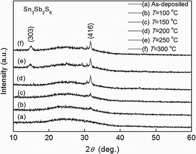
Figure 1 shows the X-ray diffraction (XRD) patterns of Sn3Sb2S6 thin films prepared at the same deposition parameters and annealed at different temperatures. The identification and assignment of the phases and crystal structure from observed diffraction patterns were made by comparison of the diffraction peaks with standard diffraction peak values of 38-0826 data. Figure 1 shows that crystalline modifications depend upon annealing temperatures which is proved for many other materials [18]. The annealing temperature 150 ° C acted as a transition stage of recrystallization and showed very poor crystalline structure. This result was found by others researchers in similar compounds [15]. Diffraction patterns of the films annealed at 200 ° C showed a peak of orthorhombic Sn3Sb2S6 phase with (416) reflection at 31.70° . When we increased annealing temperature to 250 ° C, additional peak appeared to be at 14.84° with (303) reflection. This peak corresponds to the Sn3Sb2S6 phase. In addition, annealing temperatures affect the peaks’ intensities. In fact, they are less at lower annealing temperatures while become higher with increased temperatures. Indeed, the crystallinity of the films increases by increasing the annealing temperature. This result was found by others researchers for many compounds [19, 20]. It is also noticed that no oxides phases were detected. By comparison, the SnSb2S4 and Sn2Sb2S5 thin films prepared in the same conditions we note the presence of the Sb2O4 as secondary phase [21, 22].
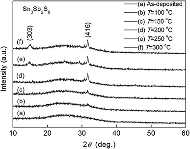 | Fig. 1 XRD patterns of Sn3Sb2S6 thin films as-deposited and annealed at different temperatures |
3.1.2 Microstructural Parameters
The crystallite size of Sn3Sb2S6 thin films was calculated from the (416) peaks using Scherrer’ s formula [23]:

where λ is the X-ray wavelength, β is the full width at half maximum (FWHM) measured in radian and θ is the Bragg angle. In the higher annealing region (250-300 ° C) crystallites grew bigger in size with comparison with lower annealing temperature (200 ° C). This behavior is proved by many other studies [24, 25] and is a characteristic of recrystallization and reorientation of planes.
The dislocation density (δ ), defined as the length of the dislocation lines per unit volume of crystal, is evaluated using the formula [26]:

where L is a factor that equals unity when the dislocation density is minimum and D is the crystallite size.
The lattice strain ε was calculated by using the Scherrer’ s relation [23]:

The stacking fault probability α , which is defined as the fraction of the layer that undergoes stacking sequence faults in a given crystal, is given by [27]:
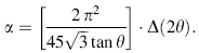
The stacking fault probabilities were calculated from the shift of the peaks of the X-ray lines of the films with reference to the 1997 JCPDS database No: 38-0826 using Eq. (4).
The microstructural parameters are given in Table 1. The crystallite size and the stacking fault probabilities increase, but the dislocation density and the strain decrease by increasing the annealing temperature. The decrease in the strain indicates the formation of higher quality film at higher temperature [28, 29]. The stacking fault probability rise is probably related to the variation in the interplanar spacing and the stresses built up in the film [30].
| Table 1 Estimated values of the microstructural parameters of Sn3Sb2S6 thin films annealed at different temperatures |
3.2.1 Transmittance and Reflectance Spectra
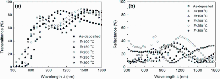
Figure 2a, b shows the optical transmittance spectra T and reflectance spectra R of Sn3Sb2S6 thin films at normal light incident in the wavelength range 300-1800 nm.
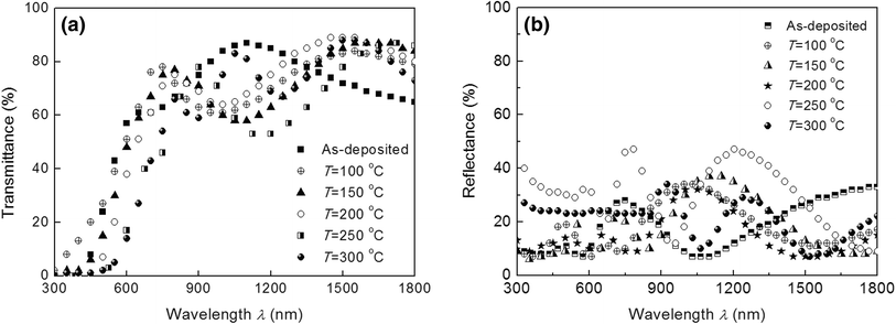 | Fig. 2 Transmittance a and reflectance spectra b of Sn3Sb2S6 thin films as-deposited and annealed at different temperatures |
It is seen that the interference effects disappear in the region of very strong absorption, while the maximum amplitude is observed in the transparent region. It should be also seen that for all thin films in the transparent region, almost R + T = 1, which falls within the experimental error which indicates no scattering or absorption in this region. These results proved the homogeneity of the deposited films [31].
3.2.2 Absorption Coefficient, Energy Band Gap and Extinction Coefficient
The optical absorption coefficient α of the investigated films is evaluated from the experimental data of transmittance and reflectance in strong absorption region using the relation [32]:
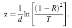
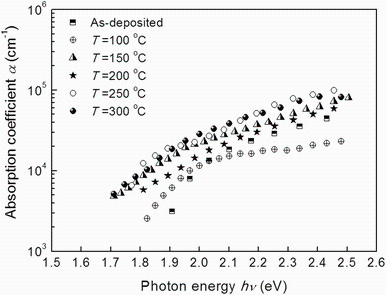
where α is the absorption coefficient and d is the film thickness, R and T are the reflection and transmission coefficients, respectively. Figure 3 shows the absorption coefficients versus the photon energy for the thin films annealed at different temperatures.
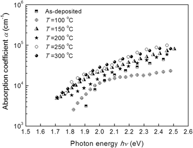 | Fig. 3 Absorption coefficient spectra of Sn3Sb2S6 thin films as-deposited and annealed at different temperatures |
The low wavelength absorption data for the deposited Sn3Sb2S6 thin films are related to the fundamental absorption, which refers to the band-to-band transition, i.e., to the excitation of an electron from the valence band to the conduction band. It can be seen that all the films have relatively high absorption coefficients (105 cm-1) in the visible and near-IR spectral range.
The fundamental absorption can be used to determine the nature and value of the optical band gap. The absorption coefficient α can be related to the energy gap Eg by applying the model postulated by Davis and Mott [33]:
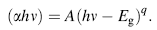
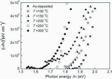
where A is a constant, h is the Planck constant, ν is the frequency of the incident beam and q is equal to ½ to a direct gap. To determine the possible transitions, we plot (α hν )2 versus photon energy hν (Fig. 4). These plots indicated that, in photon energy range 1.5-2 eV, a linear plot is obtained corresponding direct optical transition [16]. The band gap values decrease with the increase in annealing temperature (in the range 1.92-1.71 eV). The effect of the annealing on the band gap values is proved for many other compounds [25]. It may be related to the improvement in crystallization of the thin films [34].
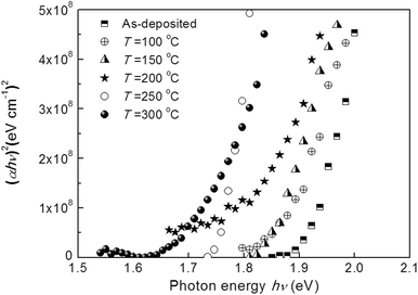 | Fig. 4 Plots of (α hν )2 versus hν for Sn3Sb2S6 thin films as-deposited and annealed at different temperatures |
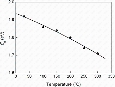
Figure 5 shows the variation in the estimated band gap values of the films with the different temperatures. The direct band gap values decrease with the increase in the temperatures which are comparable to those reported by Arbi et al. [16]. The dependence of the direct band gap Eg on the temperature can be fitted to a second-degree polynomial function:
The extinction coefficients k(λ ) of Sn3Sb2S6 thin films were calculated using the following expression [35]:
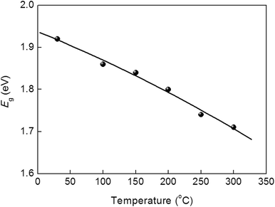 | Fig. 5 Variation in Eg with the temperature of annealing for the Sn3Sb2S6 thin films |
Figure 6 shows the dependence of k on the wavelength for Sn3Sb2S6 thin films. The extinction coefficient decreases with the increase in the wavelength showing the decrease in the fraction of light lost due to scattering and absorbance [36]. In addition, the optical absorption edge can be seen clearly for all thin films.
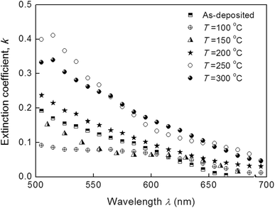 | Fig. 6 Variation in the extinction coefficient, k with wavelength for Sn3Sb2S6 thin films as-deposited and annealed at different temperatures |
3.2.3 Optical Refractive Index, n
Due to the existence of the interference patterns, the method of Swanepoel was used to calculate the refractive index n from the relation [37, 38]:
Here ns is the refractive index of the glass substrate.
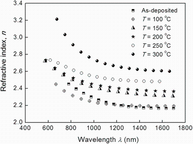
Tmax and Tmin are the values of the envelope at the wavelengths where the upper and lower envelops and the experimental transmittance spectrum are tangential. Figure 7 shows that for all the investigated samples, the refractive index decreases sharply at the wavelength of 700 nm, which is corresponding to the optical band gap of this material and becomes fairly flat above 1000 nm showing normal dispersion behavior. It is also noted that the magnitude of refractive index increases notably with increasing the annealing temperature. The observed refractive index values are in good agreement with the reported values of others Sn-Sb-S thin films prepared in the same conditions [21].
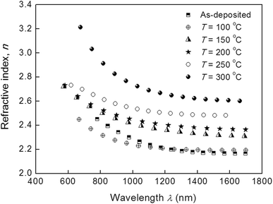 | Fig. 7 Variation in the refractive index with wavelength for Sn3Sb2S6 thin films as-deposited and annealed at different temperatures |
3.2.4 Refractive Index Dispersion Analysis
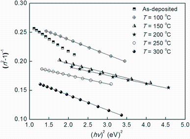
Refractive index dispersion data below the interband absorption edge were analyzed using a single-effective-oscillator fit proposed by Wemple [39]:
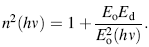
where hν is the photon energy, Eo is the oscillator energy and Ed is the dispersion energy. Ed is a measure of the average strength of the interband optical transitions, and Eo defines the average energy gap usually considered as the energy separation between the centers of both the conduction and the valence bands. The values of Ed and Eo are obtained from the intercept and the slope resulting from the extrapolation of the curve of Fig. 8. This curve represents plots of (n2 - 1) -1 versus (hν )2 [40]. All the results determined from the optical models are summarized in Table 2. It was noted that Eo decreases with increasing the annealing temperature from 100 to 250 ° C which can be related to the observed shift of the optical transmission spectra in the short wavelength region, which in turn shifts the absorption edge toward lower energies.
 | Fig. 8 Plots of (n2 - 1)-1 versus (hν ) 2 for Sn3Sb2S6 thin films as-deposited and annealed at different temperatures |
| Table 2 Estimated values of the optical parameters of Sn3Sb2S6 thin films annealed at different temperatures |
The oscillator energy Eo and the interband optical strength Ed are related to the moments of the dispersion spectra M-1 and M-3 by the relations [41]:


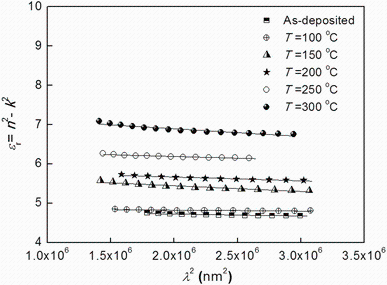
The dependence of the refractive index n on the real dielectric constant is given by the Spitzer-Fan model [42]:
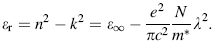
where ε ∞ is the high frequency dielectric constant in the absence of any contribution from free carriers, N/m* is the ratio of the carrier concentration to the effective mass, c is the speed of light and e is the electronic charge.
The values of ε ∞ and N/m* were deduced from the extrapolation of the plots of ε r versus λ 2 to λ 2 = 0 and from the slope of the graphs (Fig. 9). These values are listed in Table 2. It can be seen that ε r increases with the annealing temperature.
 | Fig. 9 Plots of ε r versus λ 2 for Sn3Sb2S6 thin films as-deposited and annealed at different temperatures |
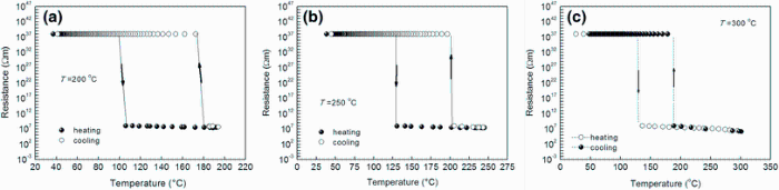
3.3.1 Resistivity Measurements
The electrical properties of the thin films are required for the optimization of the preparation conditions to use it in several applications. Electrical characterization of the films annealed at different temperatures was carried out using gold contact. Experimental observations of the thin films resistivity behavior on heating and cooling at different annealing temperatures are detailed. Figure 10a-c shows that the films regained its original resistances, forming a closed hysteresis loop [43], on the completion of the heating-cooling cycle. We found that this result is also for the SnSb2S4 and Sn2Sb2S5 thin film materials of the same family [21, 22]. The resistivity decreases with increasing temperature indicating the semiconducting nature of Sn3Sb2S6thin films. The area enclosed by the loop was found to depend on the maximum temperature to which the thin film was heated. In fact, it decreases by rising the annealing temperature which is probably related to the structural changes.
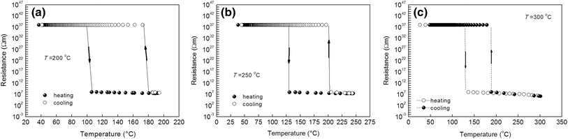 | Fig. 10 Variation in the resistivity with the annealing temperatures for the Sn3Sb2S6 thin films annealed at 200 ° C a, 250 ° C b, 300 ° C c |
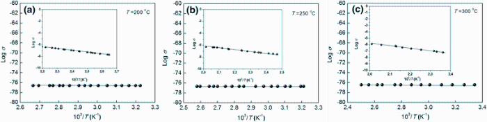
3.3.2 Activation Energy
The analysis of defects in Sn3Sb2S6 thin films was carried out by an examination of activation energy obtained using the relation [44]:
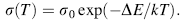
where σ 0 is a parameter depending on the semiconductor nature, k is the Boltzmann constant and Δ E is the thermal activation energy.
The electrical conductivity as a function of inverse of the temperature of annealed samples is shown in Fig. 11a, b. From the slopes of these graphs, two activation energies are determined. Δ E1 corresponds to the intrinsic region, and Δ E2 is probably related to the impurity scattering region [45]. As shown in Table 3, in the higher annealing region (250-300 ° C) Δ E1 rises while Δ E2 decreases with increasing temperature by comparison with lower annealing temperature (200 ° C). These results are in good agreement with structural study and indicate that this variation is related to the improvement in crystallization.
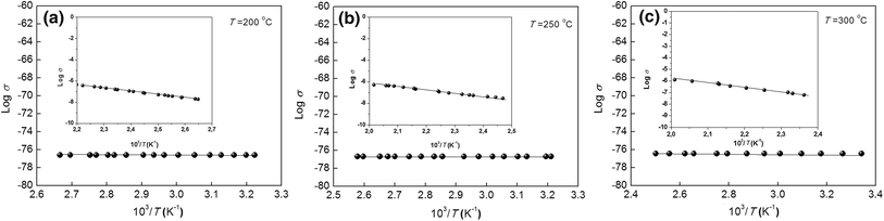 | Fig. 11 Plots of ln σ versus 103T103T for the Sn3Sb2S6 thin films annealed at 200 ° C a, 250 ° C b, 300 ° C c |
| Table 3 Estimated values of the activation energies of Sn3Sb2S6 thin films annealed at different temperatures |
Sn3Sb2S6 powder has been successfully synthesized by the horizontal Bridgman method. Thin films have been deposited on non-heated glass substrates by vacuum thermal evaporation method. The as-deposited thin films were annealed in air for 1 h at temperatures in the range 100-300 ° C. XRD results reveal that annealing affects the crystallinity and the microstructural parameters of the thin films. The Eg values decreased, whereas the refractive index n of the films raised by increasing the annealing temperature. The layers annealed at temperatures > 150 ° C undergo abrupt changes in their electrical properties and exhibit a resistive hysteresis behavior. These properties confer to the material interest perspectives for its application in diverse advanced technologies such as photovoltaic applications and optical storage.
The authors have declared that no competing interests exist.
| [1] |
|
| [2] |
|
| [3] |
|
| [4] |
|
| [5] |
|
| [6] |
|
| [7] |
|
| [8] |
|
| [9] |
|
| [10] |
|
| [11] |
|
| [12] |
|
| [13] |
|
| [14] |
|
| [15] |
|
| [16] |
|
| [17] |
|
| [18] |
|
| [19] |
|
| [20] |
|
| [21] |
|
| [22] |
|
| [23] |
|
| [24] |
|
| [25] |
|
| [26] |
|
| [27] |
|
| [28] |
|
| [29] |
|
| [30] |
|
| [31] |
|
| [32] |
|
| [33] |
|
| [34] |
|
| [35] |
|
| [36] |
|
| [37] |
|
| [38] |
|
| [39] |
|
| [40] |
|
| [41] |
|
| [42] |
|
| [43] |
|
| [44] |
|
| [45] |
|