
Substrate Temperature-Dependent Physical Properties of Thermally Evaporated Sn4Sb6S13 Thin Films
[A. Harizi1 , M. Ben Rabeh1  , M. Kanzari
2 ]
, M. Kanzari|
|


In this work, the homogenous thin films of sulfosalt Sn4Sb6S13 were successfully synthesized by the thermal evaporation technique onto corning 7059 glass substrates heated at various temperatures in the range of 30-200°C. The surface morphology and structural characteristics of Sn4Sb6S13 films were analyzed by atomic force microscopy, X-ray diffraction, and energy-dispersive X-ray, respectively. The X-ray diffraction analysis revealed that Sn4Sb6S13 thin films crystallized in monoclinic structure according to a preferential direction (
Sn x Sb y S z sulfosalt has recently attracted a great deal of attention as low-cost alternatives to conventional photovoltaic materials [1, 2]. Sn x Sb y S z combines many advantageous characteristics for optoelectronic applications, such as a suitable band gap (1-1.5 eV), a high optical absorption coefficient (up to 105 cm-1), abundant elements, and a relatively low toxicity. In addition, Sn x Sb y S z films have promising thermoelectric properties [1, 3, 4] and present particular interest as phase-change memory devices [1, 5]. Semiconducting band gaps of sulfosalt were reported by Abdelkader et al. [6], Fadhli et al. [7], Dittrich et al. [2], Boldish et al. [8], and Lomelino [9]. Fadhli et al. [7] have prepared Sn2Sb2S5 thin films by thermal evaporation and studied the effect of heat treatment in air on the properties of this material. They have shown that the as-deposited Sn2Sb2S5 sample is crystallized in spite of low substrate temperature (room temperature) and the optical properties are strongly improved. Numerous sulfosalt compounds are studied and have band gaps close to the optimum value of 1.4 eV for single-junction energy conversion from the solar spectrum [2] indicating a possible application of sulfosalt in thin-film solar cells. The solar cells were prepared using the standard Cu(In, Ga)Se2 thin-film solar cell process, i.e., Mo back contact, p-type Sn-Sb-S sulfosalt absorber layer, CdS buffer layer, and n-type ZnO window layer. Sulfosalt materials were prepared by adopting various methods such as sonochemical synthesis [10], radio frequency (RF) sputtering [1], sputtering + therm. ann. CBD [2], pulsed laser deposition [11], spray pyrolysis [12], and vacuum evaporation [7, 13]. In our previous researches [6, 7, 13], we have succeeded to synthesize SnSb4S7, SnSb2S4, Sn3Sb2S6, Sn2Sb2S5, Sn2Sb6S11, and Sn4Sb6S13 films by single-source thermal vacuum evaporation. Sn4Sb6S13 is an alternative ternary sulfosalt with high potential for photovoltaic. The aim of this work is to study the effect of substrate temperature on the structural and optical properties of Sn4Sb6S13 thin films grown by vacuum evaporation. In addition, it is intended to establish the optimized experimental substrate temperature to prepare Sn4Sb6S13 samples with high crystallinity, to assess the potential of this compound and to be used as solar cell absorber. To the best of our knowledge, no report devoting to the preparation of Sn4Sb6S13 with different substrate temperatures has been published to date.
The vacuum thermal evaporation method was used to deposit Sn4Sb6S13 film on corning 7059 glass substrates (10 mm × 20 mm × 1 mm). In our previous researches [6, 7, 13], stoichiometric amounts of the elements of 99.999% purity Sn, Sb, and S via Bridgman method have succeeded the synthesis of Sn x Sb y S z sulfosalt ingots materials. Crushed powders of these ingots were used as a raw material for the thermal evaporation. Thin films of Sn4Sb6S13 were sublimated by conventional thermal evaporation technique using high vacuum coating system (Model Alcatel). The evaporator system utilizes two pumps to evacuate the high vacuum chamber, which was made of an enclosed bell jar. Powder of Sn4Sb6S13 was used as the evaporation source material. The substrates were placed directly above the source at a distance of 15 cm. The vacuum chamber was evacuated to 1.33× 10⁻⁴ Pa (10-6 Torr) before the source was heated. The molybdenum boat was heated using 40 A direct current for 10 s to melt the Sn4Sb6S13. The current was increased slowly to 90 A until all of the Sn4Sb6S13 evaporated. The films were removed after waiting for a few hours for the chamber to cool down. The films were deposited onto clean corning 7059 glass substrates for optical measurements; the corning 7059 glass substrates were carefully cleaned by chromic acid for 15 min and then rinsed by deionized water. The material was sublimated from a heated molybdenum boat in a vacuum of 1.33 × 10⁻³ Pa (10-5 Torr). The substrate temperature controlled by a chromel-alumel thermocouple was varied from 30 to 200 ± 5° C. Substrate heating was performed by an electrical heater. The optimized deposition parameters such as molybdenum boat-substrate distance (10 cm) and evaporation time (20 min) were kept constant. In the end of the evaporation process, the heater was slowly closed, and the glass substrates were given up cooling for 1 h in vacuum. For each substrate temperature, the structure, morphological, and optical properties of the produced films were investigated.
The crystal structures of the samples were analyzed using a Philips X’ Pert X-ray diffractometer in Bragg-Brentano geometry (θ /2θ ) with CuKα radiation (λ = 0.154056 nm and 40 kV, 30 mA) in the range 2θ = 20° -70° . The surface morphology of the films was investigated using the atomic force microscopy (AFM, Vecco model D 3100). The transmittance T(λ ), the reflectance R(λ ), and the spectra of Sn4Sb6S13 thin films were measured at normal incidence of light in the spectral range 300-1800 nm using a double-beam spectrophotometer (SHIMDZU model UV 3100S). An uncertainty of 1% was given by the manufacturer for measurements obtained by this spectrophotometer. A glass substrate, such as that used for thin film deposition, was used as a reference for transmittance and reflectance scan. Film thickness was calculated from the positions of interference maxima and minima of reflectance spectra using a standard method [14]. The film thickness was controlled and monitored during the evaporation process by using a quartz crystal sensor (Model, TM-350 MAXTEK, Inc., USA). The deposited films have a thickness in the wavelength range 400-540 nm.
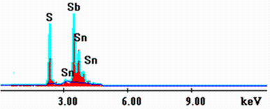
Energy-dispersive X-ray (EDX) analysis was used to determine the elements composition in typical Sn4Sb6S13 thin film. The result is shown in Fig.1. The spectrum of the film deposited at Ts = 30° C shows only S, Sn, and Sb elements, indicating the purity of the synthesized film. This result provides the elemental composition and the average atomic percentage of the Sn4Sb6S13 film deposited at Ts = 30° C, showing a high average atomic percentage of S (54.4%) compared to both Sn and Sb (12.8% and 32.8%).
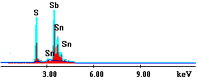 | Fig.1 EDX measurements of the Sn4Sb6S13 thin films deposited at 30° C |
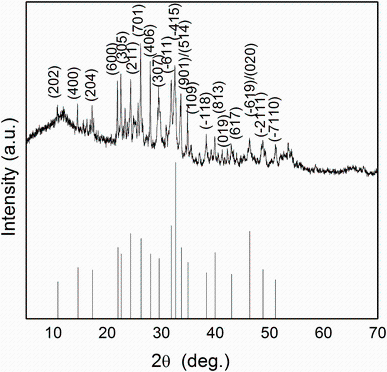
3.2.1 Powder X-ray Diffraction
The powder profile of Sn4Sb6S13 material is shown in Fig.2. The pattern exhibits well sharp and intense peaks, which is a signature of crystalline phase of prepared Sn4Sb6S13. The powder X-ray diffraction data are indexed to be a monoclinic crystal system. The lattice parameters a, b, c, and β are calculated by using the following relation:
 | Fig.2 X-ray diffraction patterns of standard and as-synthesized Sn4Sb6S13 powder |
The corresponding lattice cell parameters are evaluated: a = 2.438 nm, b = 0.392 nm, c = 2.288 nm, and β = 91.19° . These results are in good agreement with those in JCPDS Card No. 74-0676 (a = 2.431 nm, b = 0.391 nm, c = 2.349 nm, and β = 94.05° ). The peak positions shown in Fig.2 match well with those in the standard pattern (JCPDS Card No. 74-0676).
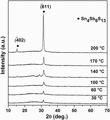
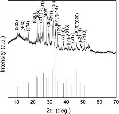
3.2.2 X-ray Diffraction of Sn4Sb6S13 Films
Figure 3 shows the XRD patterns of a Sn4Sb6S13 thin film at various substrate temperatures. The reflections illustrate a strong peak of Sn4Sb6S13, corresponding to the
 | Fig.3 X-ray diffraction patterns of Sn4Sb6S13 thin films deposited on glass substrates heated at different temperatures |
where k is a constant (a shape factor whose value is about 0.9), λ is the wavelength of X-ray radiation (0.15405 nm) used, β is the full width at half maximum (FWHM) intensity of the diffraction line, and θ is the diffraction angle. By increasing substrate temperature from 30 to 200° C, we note that the crystallite sizes of the samples increase from 20 to 48 nm and the FWHM of the (
The lattice strain values were in the range of 6.38 × 10⁻⁴-2.65 × 10⁻⁴. We remark that the micro-strain decreases with increasing substrate temperature. This change may be explained by the decrease in concentration of lattice imperfections related to the growth in the grain size.
The dislocation density (δ ) is defined as the length of dislocation line per unit volume of crystal. It was calculated from the formula [17]:
The calculated dislocation density varied in the range of 25 × 1014-4.33 × 10¹⁴ (lin. m-2) and is decreasing with increasing substrate temperature. This result indicates that the layers become more relaxed due to reduction in defects in the structure. This suggests the improvement in film crystallinity by increasing substrate temperature. The number of crystallites per unit area can then be evaluated using the following relation [18]:
where t is the film thickness. The estimated number of crystallites per unit area is varied between 67.2 × 10¹⁵ and 3.6 × 10¹⁵ per unit area with substrate temperature. This increase can be attributed to grain agglomeration. First, at low substrate temperature, the Sn4Sb6S13 thin films are composed of large number of small grains. Then, by increasing substrate temperature the small grains become greater. The calculated values of microstructural parameters are summarized in Table 1. It is clearly observed that substrate heat treatments improve the crystallinity of films.
| Table 1 Structural parameters and surface roughness of Sn4Sb6S13 films deposited at different substrate temperatures |
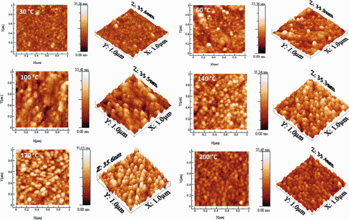
3.2.3 AFM Analysis
Figure 4 shows two-dimensional (2D) and three-dimensional (3D) surface morphology images of Sn4Sb6S13 thin films deposited at different substrate temperatures. The scanning area was 1.0 μ m × 1.0 μ m in tapping mode. The root-mean-square roughness (RMS) and the grain size were determined by using standard software (WS × M 5.0 software) [19]. It is clearly observed that the films deposited at various temperatures showed different surface roughnesses. The films deposited at room temperature and at 60° C show a dense and smooth surface due to poor crystallinity. However, at substrate temperature higher than 100° C the surface becomes homogeneous and constituted of densely packed grains. The crystallites have spherical form and uniform distribution. The AFM measurements indicate that the RMS of all samples increases from 2.81 to 8.23 nm. This is caused by the rise in substrate temperature from 30 to 200° C (Table 1). The surface roughness of the films was also evaluated by using an optical method based on the spectrophotometric data following this formula (σ ≪ λ ) [20]:
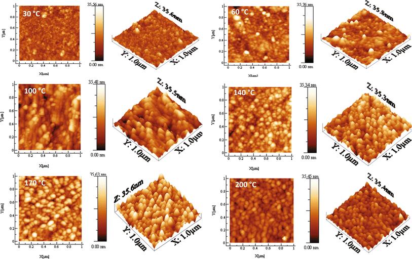 | Fig.4 2D and 3D AFM micrographs (1μ m × 1 μ m) of Sn4Sb6S13 thin films deposited on glass substrates heated at different temperatures |
where RS is the specular reflection, RT is the total reflection of the films, and σ , μ are the average roughness of the irregularities, respectively, the highest and the lowest. The total reflection RT equals the sum of RS and Rdiff (diffuse reflection). The diffuse and the specular reflection data of Sn4Sb6S13 films were measured by a UV-visible-NIR spectrophotometer in the spectral range of 300-1800 nm. Equation (6) is formed by two terms. The first defines the coherent part of reflection, while the second term represents the incoherent part. If the second term is negligible, a new expression of the relation (7) is obtained [21]:
where A is a constant from the spatial fluctuations of the optical constants. Thus, by plotting ln(RS/RT) versus
3.3.1 Optical Transmittance and Reflectance Spectra
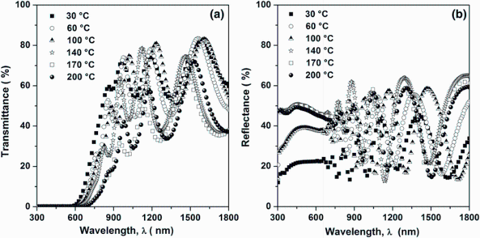
Figure 5a, b shows the typical transmittance T(λ ) and reflectance R(λ ) spectra of Sn4Sb6S13 thin films grown at different substrate temperatures in the wavelength range of 300-1800 nm. It is clear that all films exhibit two distinct slopes. The first one (900-1800 nm) is commonly named the transparency zone in which multitude interference fringes are seen showing fairly homogenous films. In this region, all films exhibit a good transparency (70%-80%) in the visible and infrared regions. However, a small decrease in the transmission by increasing the substrate temperature was observed in the spectral range 900-1800 nm. The second region (300-900 nm) is well known by the zone of high absorption. In this spectral region, the signal is strongly reduced at the band edge, especially at 200° C. In this spectral range, an increase in the rate values of reflection of 30% for substrate temperature of 200° C was also observed, which can be explained by a decrease in the absorption phenomena reducing the performance of this material in this region.
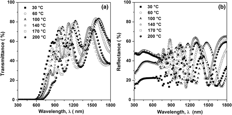 | Fig.5 Optical transmission a and reflection b spectra of Sn4Sb6S13 thin films deposited on glass substrates heated at different temperatures |
3.3.2 Absorption Coefficients, Energy Gap, and Refractive Index
The optical absorption coefficient was evaluated from the transmittance T(λ ) and reflectance R(λ ) data by using the following formula [22, 23]:
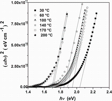
where d is the film thickness. Figure 6 shows the dependence of the absorption coefficient on photon energy for Sn4Sb6S13 films deposited at different substrate temperatures. It can be seen that all the Sn4Sb6S13 films have relatively high absorption coefficients which are higher than 105 cm-1 in the visible and the near-IR spectral regions. This result is very important because the spectral dependence of the absorption coefficient affects the solar cell conversion efficiency in photovoltaic applications. The dependence of the absorption coefficient on photon energy is analyzed in the high absorption regions to achieve detailed information about the energy band gaps. The absorption coefficient and photon energy can be related by applying the model postulated by Tauc [24], Davis and Mott [25] independently:
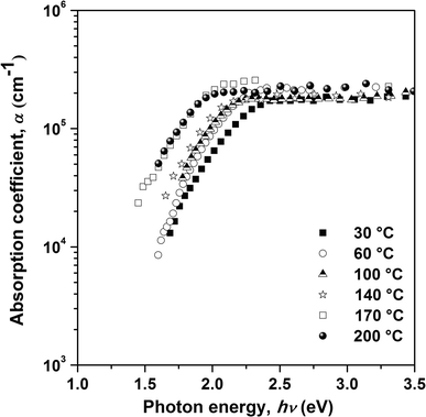 | Fig.6 Absorption coefficient α of Sn4Sb6S13 thin films deposited on glass substrates heated at different temperatures |
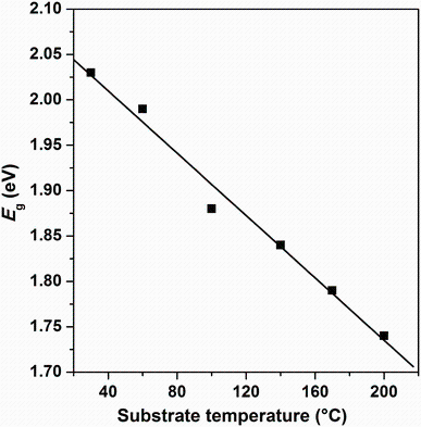
where A is a constant, Eg is the optical band gap, h is the Planck constant, and n is an index that characterizes the optical absorption process. In theory, n equals 1/2, 2, 3, and 3/2 for indirect allowed, direct allowed, indirect forbidden, and direct forbidden transition, respectively. In Fig.7, (α hν )2 versus hν is plotted in order to extract direct band gap values by extrapolating the linear regions of (α hν )2 to the horizontal photon energy axis. The direct band gap energy tends to decrease from 2.03 to 1.69 eV with increasing substrate temperature. Figure 8 shows the variation of optical band gap Eg versus substrate temperature. The decrease in Eg to 1.69 eV by increasing substrate temperature may be explained by the enhancement of crystallite size and the decrease in defects [2]. This result was proved by many other studies of Sn3Sb2S6, SnSb4S7, and Sn2Sb6S11 deposited by the same technique and in the same condition [26, 27]. Due to the existence of the interference patterns, this exhibits several maxima and minima as the wavelength increases, and the method of Swanepoel [28, 29] was used to calculate the refractive index n. The method is based on the approach of Manifacier et al. [30]. This approach offers a creation of upper and lower envelope for transmission spectrum beyond the absorption edge. The refractive index can then be calculated from the relation [28, 29]:
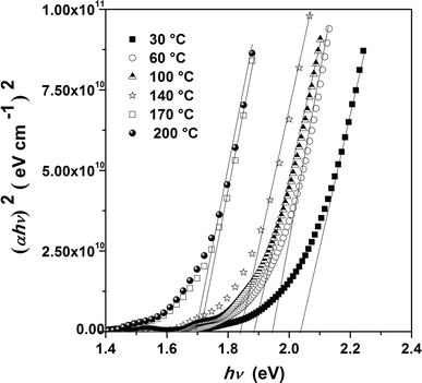 | Fig.7 Plot of (α hν )2 versus photon energy (hν ) for Sn4Sb6S13 thin films deposited on glass substrates heated at different temperatures |
 | Fig.8 Variation of band gap energy Eg versus substrate temperature for Sn4Sb6S13 thin films |
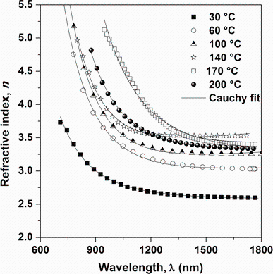
where ns is the refractive index of glass substrate. TM and Tm are the values of the envelope at the wavelengths where the upper and lower envelops and the experimental transmittance spectrum are tangential, respectively. The variations of refractive index n versus wavelength of the Sn4Sb6S13 films deposited at different substrate temperatures are shown in Fig.9. As observed, the refractive index is influenced by substrate temperature and shows normal dispersion behavior. Indeed, n decreases with increasing wavelength of incident photon and tends to be constant at higher wavelengths. The dispersion spectra of refractive index were fitted using the Cauchy formula [31]:
 | Fig.9 Variation of refractive index n vs wavelength and the fit with Cauchy’ s formula for Sn4Sb6S13 thin films deposited at different substrate temperatures |
where A and B are the Cauchy’ s parameters and λ is the wavelength of light used. For λ → ∞ , the significance of the n0 appears immediately as n∞ . Figure 9 shows the variation of n with Cauchy fitting for as-deposited Sn4Sb6S13 thin films at different substrate temperatures. It is clear that the values of n for all the investigated samples obey the Cauchy law. The values of fit parameters and n0 are presented in Table 2. There is a good correlation between refractive index and optical band gap of semiconductors, where typically, n increases as Eg decreases. The same result is obtained by others study of SnSbS thin films grown by vacuum evaporation method [7]. Since Eg decreases with substrate temperature, the temperature dependence of n arises from the variation of Eg with the substrate temperature which can be correlated to the improvement in film crystallinity. Therefore, energy band gap decreases and refractive index increases with decreasing substrate temperature, which can be related to the film crystallization [32]. The refractive index dispersion has an important role in the research for optical materials due to a significant factor in optical communication and in designing devices for spectral dispersion. The dispersion was analyzed using the model of single oscillator and can be expressed by the Wemple-DiDomenico relationship as follows [33, 34]:
| Table 2 Results concerning Cauchy parameters and refractive index n(0) at zero photon energy |
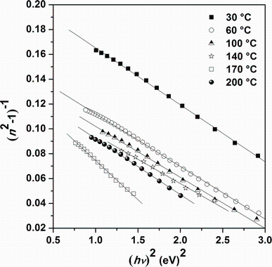
where hν is the photon energy, n is the refractive index, E0 is oscillator energy, and Ed is the dispersion energy. Ed allows evaluating the average force inter-band optical transition. Wemple and DiDomenico have related this parameter to the coordination number for anion and the valence electron number per anion. E0 and Ed values are obtained from the intercept E0/Ed and the slope (E0Ed)-1by extrapolating the curve representing the plot of (n2-1)-1 versus (hν )2 (Fig.10). The refractive index n(0) at zero photon energy, which is defined by the infinite wavelength dielectric constant, can be deduced from the dispersion relationship by extrapolation of the linear part (n2-1)-1 versus (hν )2. The values of n0 found by the Cauchy fitting and the Wemple-DiDomenico model are in good agreement. Dielectric constants are linked to the refractive index n and allow us to further analyze the optical properties of samples. The dependence of refractive index n on the real dielectric constant is expressed by the Spitzer-Fan model [35]:
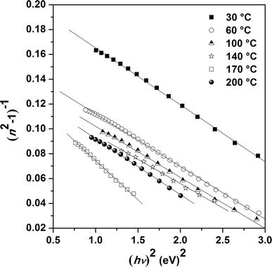 | Fig.10 Plot of (n2-1)-1 versus (hν )2 for Sn4Sb6S13 thin films deposited at different substrate temperatures |
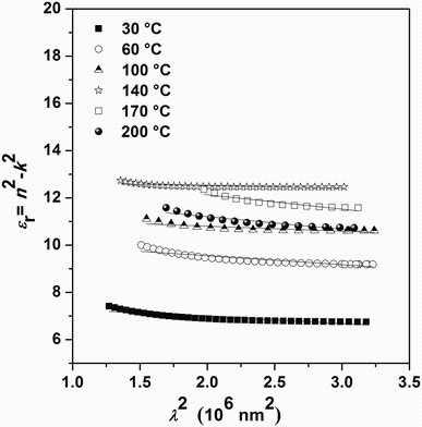
ε r=n2-k2=ε ∞ -
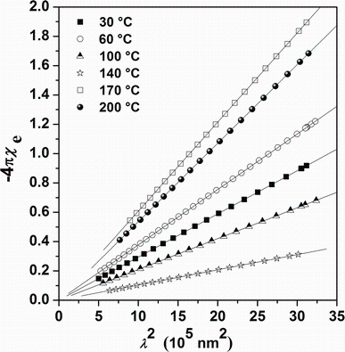
where ɛ ∞ is the high-frequency dielectric constant in the absence of any contribution from free carriers, N/m* is the ratio of the carrier concentration to the effective mass, c is the speed of light, and e is the electronic charge. ɛ ∞ and N/m* were deduced from plotting ε r. versus λ 2 (Fig.11) and fitting to a straight line. It is important to compare the values of ɛ ∞ achieved from the Wemple-DiDomenico model (Fig.10) with that obtained from the Spitzer-Fan model (Fig.11). Indeed, the two models show satisfactory agreement. On the other hand, the electrical susceptibility χ e owing to the inter-band transitions of free carriers can be obtained from the optical constants and is determined as:
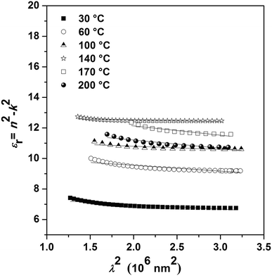 | Fig.11 Plot of ε r versus λ 2 for Sn4Sb6S13 thin films deposited at different substrate temperatures |
Plots of
 | Fig.12 Plot of |
| Table 3 Values of the dispersion energy (Ed), oscillator energy (E0), ratio of the carrier concentration to the electron effective mass (n/m* ), the lattice dielectric constant (ε ∞ ), and electrical susceptibility |
Sn4Sb6S13 thin films were successfully evaporated on heated glass substrate by vacuum evaporation method. The substrate temperatures were varied in the range of 30-200° C. From the powder X-ray diffraction study, it was observed that prepared material belongs to monoclinic crystal system and the corresponding lattice cell parameters are evaluated: a = 2.438 nm, b = 0.392 nm, c = 2.288 nm, and β = 91.19° . X-ray diffraction analyses showed that the as-deposited Sn4Sb6S13 films have a polycrystalline structure. All films are oriented along the (
The authors have declared that no competing interests exist.
作者声明: 无竞争性利益关系
| [1] |
|
| [2] |
|
| [3] |
|
| [4] |
|
| [5] |
|
| [6] |
|
| [7] |
|
| [8] |
|
| [9] |
|
| [10] |
|
| [11] |
|
| [12] |
|
| [13] |
|
| [14] |
|
| [15] |
|
| [16] |
|
| [17] |
|
| [18] |
|
| [19] |
|
| [20] |
|
| [21] |
|
| [22] |
|
| [23] |
|
| [24] |
|
| [25] |
|
| [26] |
|
| [27] |
|
| [28] |
|
| [29] |
|
| [30] |
|
| [31] |
|
| [32] |
|
| [33] |
|
| [34] |
|
| [35] |
|
| 36 |
|