Search for articles:
Lin Jiang
Corresponding authors:
Received: 2018-10-20
Revised: 2018-12-2
Online: 2019-11-05
Copyright: 2019 Editorial board of Acta Metallurgica Sinica(English Letters) Copyright reserved, Editorial board of Acta Metallurgica Sinica(English Letters)
More
Abstract
Target assembly is a key consumable material for producing thin film used in the electronic packaging and devices. The residual stresses induced during the process of soldering are detrimental to the performance of target assembly. In this work, the intensity and distribution of the soldering residual stress of Co/In/Cu target assembly subjected to a 20 W/(m2 K) cooling condition corresponding to the actual air cooling process were studied, based on finite element simulation and Taguchi method, to optimize the sputtering target assembly. Effects of different control factors, including solder material, thickness of solder layer, target and backing plate, on the soldering residual stress of target assembly are investigated. The maximum residual stress is calculated as 9.28 MPa in the target located at 0.16 mm from target-solder layer interface and at a distance of 0.78 mm from symmetry axis. The optimal design in target assembly has the combination of indium solder material, cobalt target at 12 mm thick, solder layer at 0.8 mm thick, copper backing plate at 15 mm thick. Moreover, solder material is the most important factor among control factors in the target assembly.
Keywords:
Nowadays, the major trends in the electronic packaging are more functionality, smaller size, thinner packages and higher density, which requires film to be thinner and thinner [1, 2, 3, 4, 5]. Cobalt film as magnetic film has been widely used in electronic devices. However, the thinner the cobalt film fabricated on devices, the greater the effects of microstructure and thickness uniformity on the performance of film. Therefore, it is a new challenge for the materials used in the electronic packaging and semiconductors, whereas accompanying the development of electronic information, films have been used in electronic devices more and more widely such as barrier films and interconnect films and have significant impact on the performance of the integrated circuit [6]. Thus, the demand of thin film material is increasing dramatically and the production of thin film material is urgently needed [7, 8, 9, 10]. However, the microstructure and thickness uniformity of cobalt film on devices are closely related to the residual stress of sputtering target assembly which is a key consumable material for producing thin film during fabrication.
Generally, sputtering target assembly is always attached to backing plates to lower cost, to increase mechanical rigidity and to improve target cooling efficiency [11]. However, target and backing plate are usually two different materials with different coefficients of thermal expansion (CTE), so there are soldering residual stresses which can linger inside materials due to internal strain incompatibility, which can cause failures including desoldering and bucking deformation in sputtering target assembly. Moreover, desoldering and bucking deformation are detrimental to sputtering performance of target assembly and to the quality of thin film, such as thickness uniformity, ingredient uniformity and adhesion. Because residual stresses are so important to reliability of target assembly, the determination of residual stresses intensity and distribution are necessary.
However, since residual stresses are very complex, there are few research papers on the residual stresses in target assembly, and most of the attentions have been just focused on the reliability of the electronic products [12, 13, 14, 15, 16]. Generally, the stress measurement techniques can be divided into nondestructive techniques and destructive techniques according to whether specimen is destructed or not. The advantage of nondestructive measurement techniques is that there is no destruction to specimen, while the disadvantage is that it just can measure residual stress of surface or a specific distance from the surface. However, the application of nondestructive techniques is limited, including mainly X-ray diffraction, ultrasonic method and neutron diffraction [17, 18]. Destruction measurement techniques are more applicable than those of nondestructive measurement techniques, such as hole drilling method, contour method and sectioning method. Destruction measurement techniques have been used for many years because of high accuracy, but they can cause destruction to specimen. Therefore, destructive measurement techniques are not applicable to expensive or nondestructive specimens [19, 20]. As a powerful method, numerical simulation with lower cost, high efficiency and flexibility characteristic is widely used for stress measurement and investigation; especially, with the development of the microelectronic industry, the microelectronic reliability is becoming more and more important and the failure of electronic device always is an issue concerning coupled physical field. The finite element method is a very useful method to solve the coupled field problems, which has been widely used in the estimation of reliability, prediction of lifetime and optimization of structure. Mei et al. [21] utilized finite element method to simulate the coupled electrical, thermal and mechanical fields in electronic devices and to assess the response of the solder joint exposed to power cycling. Lu and Jin [22] developed a multiphysics simulation technique, including electrical, thermal and mechanical fields, based on finite element method to analyze large-scale interconnect structures. The simulation of residual stress in target assembly has not been reported yet.
In this work, the intensity and distribution of residual stress induced by soldering process of Co/In/Cu target assembly were studied qualitatively using finite element method and Taguchi method. The effects of control factors including solder material, thickness of target, solder layer and backing plate on residual stress were investigated. It is imperative to optimize parameters of target assembly to enhance its reliability and performance during applications.
In this work, the simulation was carried out using the available commercial ANSYS software. The several hypotheses were made as follows: (1) Target and backing plate were soldered perfectly, that is to say, there is no unsoldered area; (2) Target and backing plate are assumed to be linear elastic in the whole process of soldering and cooling while solder layer is viscous-elastic-plastic; (3) In order to simplify the model, we have ignored cooling channel in the backing plate.
Actually, cobalt target used in the industrial production of cobalt film is usually soldered on copper backing plate with indium solder. The material properties of target and backing plate are displayed in Table 1. The properties of indium are strongly temperature dependent, as shown in Table 2 [23].
Table 1 Material properties of cobalt and copper
| Material | Thermal conductivity (W/(m K)) | CTE (10-6/K) | Young’s modulus (GPa) | Poisson’s ratio |
|---|---|---|---|---|
| Cobalt | 89.5 | 13.9 | 211 | 0.32 |
| Copper | 396.0 | 16.5 | 128 | 0.34 |
Table 2 Material properties of indium [
| Temperature (K) | 75 | 140 | 205 | 270 | 335 | 400 |
|---|---|---|---|---|---|---|
| Poisson’s ratio | 0.3 | |||||
| Young’s modulus (GPa) | 19.11 | 17 | 14.89 | 12.78 | 10.66 | 8.55 |
| CTE (10-6/K) | 23.9 | 26.9 | 28.27 | 30.46 | 32.65 | 34.83 |
| Thermal conductivity (W/(m K)) | 99.83 | 94.37 | 89.03 | 83.82 | 78.74 | 73.78 |
Partial geometrical model of target-backing plate assembly used in this study is shown in Fig. 1a. The target (Φ450 mm × 12.7 mm) was attached to the backing plate (Φ540 mm × 12.7 mm), and the thickness of solder layer is 0.7 mm. Due to the axial symmetry of target-backing plate assembly, an arbitrary meridian plane, as shown in Fig. 1b, was selected to analyze the residual stress in target-backing plate assembly.
Fig. 1 Schematic of Co/In/Cu target-backing plate assembly with a 3D model, b 2D model
Thermal-structural coupled field was used to perform the simulation [24]. The numerical simulation process can be defined as follows:
Step 1 Create geometric model and define material properties. The complete material properties, as shown in Tables 1 and 2, were input into ANSYS software to define material models, and the geometric model was parameterized and properly established.
Step 2 Finite element model. The finite element method (FEM) model with PLANE 55 element is established for a 2D axisymmetric thermal analysis to the target-backing plate assembly, as shown in Fig. 2. And the FEM model contains 14,412 elements and 44,173 nodes. For the purpose of improvement in accuracy and precision, the fine elements were used to determine the detailed stress distribution at the area near target outer edge and solder layer.
Step 3 Apply loads and degree of freedom (DOF) constraints. In the soldering process of Co/In/Cu target assembly, the actual temperature of target’s upper surface and backing plate’s lower surface is 433 K and 453 K, respectively. So during thermal analysis, 433 K and 453 K temperature constraints are, respectively, applied on the upper surface of target and the lower surface of backing plate and steady-state nonlinear analysis is considered in the analysis. In the industrial production, the target assembly is air-cooled from welding temperature to room temperature and the convection heat transfer coefficient corresponding to air cooling is generally 20 W/(m2 K). Thus, model convection boundary conditions, 20 W/(m2 K), are applied on all surfaces, and transient nonlinear analysis is set in the analysis.
Step 4 Set load steps and temperature solution. The thermal analysis types of load step 1 and load step 2 are defined as steady-state nonlinear and transient nonlinear analysis, respectively. The temperature distribution of target-backing plate assembly, at the moment of completion soldering, can be obtained in the solution of load step 1. In the load step 2, under 20 W/(m2 K) heat convection boundary condition, target-backing plate assembly has been cooled for 30 min and the temperature results of load step 1 are defined as the initial temperature.
Step 5 Switch element and apply structural condition. After thermal analysis, we switch thermal element PLANE55 to PLANE42 for target and backing plate and VISCO106 for solder layer. Since the target-backing plate assembly is axial symmetry, the displacement constraint (UX = 0) is applied on the symmetry axis location’s nodes. Anand material model has been used to describe the rate-dependent behavior of solder alloy at high temperature. As a viscoplastic model, Anand model does not require the explicit yield condition. Therefore, the plastic flow can occur at any nonzero stress value. Besides, the model uses a single scalar internal state variable s, the deformation resistance, to measure the isotropic resistance offered by the internal state of the solder to the plastic flow. The strain hardening and softening behavior of Anand model is described by one flow equation as shown in Eq. (1) and three corresponding evolution equations as follows:
$$\frac{{{\text{d}}\varepsilon_{\text{p}} }}{{{\text{d}}t}} = A\left[ {\sinh \left( {\frac{\xi \sigma }{s}} \right)} \right]^{1/m} \exp \left( { - \frac{Q}{RT}} \right),(1)$$
$$\frac{{{\text{d}}s}}{{{\text{d}}t}} = \left\{ {h_{0} (|B|)^{a} \frac{B}{|B|}} \right\}\frac{{{\text{d}}\varepsilon_{\text{p}} }}{{{\text{d}}t}},(2)$$
$$B = 1 - \frac{s}{{s^{*} }},(3)$$
$$s^{*} = \hat{S}\left[ {\frac{{{\text{d}}\varepsilon_{\text{p}} /{\text{d}}t}}{A}\exp \left( {\frac{Q}{\text{RT}}} \right)^{n} } \right],(4)$$
where εp is the inelastic strain rate, A is a pre-exponential factor, Q is the activation energy, R is the gas constant, T is current absolute temperature, ξ is the multiplier of stress, σ is the equivalent stress, m is strain rate sensitivity of stress, s is the internal variable, h0 is the hardening/softening constant, a is the strain rate sensitivity of hardening/softening, s* is the saturation value of internal variable for a given temperature and strain rate, Ŝ is a coefficient for deformation resistance saturation value and n is the strain rate sensitivity for saturation value. What’s more, the initial value of deformation is given as S0.
Anand material model which is supported by VISCO106 element is selected for solder layer material. And it has been already widely used in reliability analysis of electronic packaging. For example, Zhang et al. [25] applied Anand material model to leader free solder joints to investigate inelastic deformation behavior of the lead-free solders. The parameters of Anand material model are shown in Table 3 [26].
Step 6 Read thermal result. The temperature results of load step 2 are defined as thermal load in the structural analysis process, and the analysis type was set to steady-state nonlinear analysis.
Step 7 Solution. Through structural analysis, the intensity and distribution of residual stresses are obtained.
Fig. 2 Finite element model (2D) of target assembly
Table 3 Material parameters of viscoplastic Anand model of solder [
| Material | S0 (MPa) | Q/R (1/K) | A (1/s) | ξ | h0 (MPa) | m | ŝ | n | a |
|---|---|---|---|---|---|---|---|---|---|
| Indium | 28.30 | 9369.7 | 2.33E8 | 49.97 | 0 | 0.300 | 28.30 | 0 | 1 |
| Sn3.0Ag0.5Cu | 40.16 | 8400.0 | 4.61E6 | 4.60 | 3090.00 | 0.162 | 14.37 | 0.038 | 1.56 |
| Sn63Pb37 | 12.41 | 9400.0 | 4E6 | 1.50 | 1378.95 | 0.303 | 13.79 | 0.070 | 1.30 |
Taguchi method has been extensively applied in quality improvement in products and manufacturing process design since it was proposed. Zhang et al. [27] used Taguchi method to analyze effects of different control factors on the solder joints reliability during thermal cyclic loads. In this work, Taguchi method as an effective way was applied to analyze the effects of solder material and thickness of target, backing plate and solder layer on the residual stress in target-backing plate assembly. And pure indium, Sn3.0Ag0.5Cu and Sn63Pb37 are selected as solder materials. Similar to the properties of indium solder described in Sect. 2.3, Anand model was also applied to Sn3.0Ag0.5Cu and Sn63Pb37, whose properties are shown in Tables 3 and 4, respectively. Orthogonal array and S/N ratio have been used in Taguchi method, where S is the intensity of signal and N is the intensity of noise. Considering the control factors and their levels, the L9(34) orthogonal array is applied in the finite element method calculation of maximum soldering residual stress. The smaller the signal-to-noise (S/N) ratio, the smaller the residual stresses are introduced in target-backing plate assembly, which means the better reliability. The S/N ratio objective function for quality characteristic of the smaller-the-better type was shown as follows:
Table 4 Material properties of Sn3.0Ag0.5Cu and Sn63Pb37
| Material | Thermal conductivity (W/(m K)) | CTE (10-6/K) | Young’s modulus (GPa) | Poisson’s ratio |
|---|---|---|---|---|
| Sn3.0Ag0.5Cu | 35.0 | 25.0 | 39.5 | 0.35 |
| Sn63Pb37 | 35.4 | 24.5 | 26.1 | 0.36 |
$$S/N = - 10\log \left( {\frac{{\sum\nolimits_{i = 1}^{r} {\mathop y\nolimits_{i}^{2} } }}{r}} \right),(5)$$
where r is the total number of measurements, yi is the ith measurement data and S/N is the signal-to-noise ratio in decibel. In this finite element simulation work, r = 1, and yi = Seqv (Seqv is von Mises equivalent stress). So, Eq. (5) can be described as follows:
$$S/N = - \;10\log \left( {\mathop s\nolimits_{\text{eqv}}^{2} } \right).(6)$$
Four control factors which contain three levels were selected in the investigation of residual stress as shown in Table 5.
Table 5 Control factors and levels
| Level factor | Solder | Target thickness | Solder layer thickness | Backing plate thickness |
|---|---|---|---|---|
| A | B | C | D | |
| Level 1 | In | 15 | 0.8 | 15 |
| Level 2 | Sn3.0Ag0.5Cu | 12 | 0.7 | 12 |
| Level 3 | Sn63Pb37 | 9 | 0.6 | 9 |
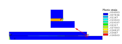
The intensity and distribution of soldering residual stresses of Co/In/Cu target-backing plate assembly are studied with the material properties as described in Sect. 2. Firstly, thermal analysis was performed to obtain distribution of temperature in the target-backing plate assembly. After soldering, the distribution of simulated temperature is shown in Fig. 3a. We find that the temperature gradient variation is along the thickness direction. And there is a large thermal drop on the target, which will introduce large thermal stress in the target. Under 20 W/(m2 K) heat convection boundary condition, target-backing plate assembly has been cooled for 30 min and the corresponding temperature distribution is shown in Fig. 3b. The temperature gradient goes in the direction of the radius. The maximum temperature (356.6 K) and minimum temperature (354.8 K) positions are at symmetry axis locations and backing plate outer edge locations, respectively. After thermal analysis, structural analysis was performed in which residual stresses were obtained as shown in Fig. 4. From Fig. 4, it easily can be found that the residual stresses at area near the interface of target and solder layer are greater than anywhere else and the maximum residual stress is 9.28 MPa in the target located at 0.16 mm from target-solder layer interface and at a distance of 0.78 mm from symmetry axis, which is indicated by black arrow in the partial enlarged figure.
Fig. 3 Distribution of temperature a at the moment of soldering completion, b after 30 min cooling
Fig. 4 Distribution of von Mises stress after 30 min cooling
Figure 5 shows the distribution of residual stress in the center of target assembly from backing plate’s lower surface to target’s upper surface, namely, from 0 to 26.1 mm. We can find the position of maximum residual stress is about 0.25 mm from the target-solder layer interface in target, which is consistent with the result of Zhu et al. [28] and coincides with the result of Ni et al. [29]. There is a characteristic of residual stress distribution in the symmetry axis that the residual stresses in both sides are larger than those in the middle of target, backing plate and solder layer. The characteristic has also been found in the other welding joints [30].
Fig. 5 Distribution of residual stress in the center of target assembly from backing plate’s lower surface to target’s upper surface
As shown in Fig. 6, the residual stresses of target-solder layer interface decrease from center position to outer edge, but concentration stress can be observed at position near the outer edge of target. We define the position of center of target-solder interface as the point 1 and the position of outer edge of target-solder interface as point 3, respectively. The middle position of point 1 and 3 is the point 2. The time histories of residual stresses of three points are shown in Fig. 7. As time goes on, the residual stresses increase obviously. Due to weaker displacement constraints, there are large strains to release the stresses as shown in Fig. 8. Therefore, although stress concentration occurs in the outer edge of lower surface of target, the residual stresses are relatively small.
Fig. 6 Distribution of residual stress in target near target/solder interface along radial direction
Fig. 7 Time history of stress
Fig. 8 Strain of target assembly after 30 min cooling
In order to obtain the optimal parameters’ combination of target-backing plate assembly including solder material and thickness of target, backing plate and solder layer, the effects of these control factors and the effects of different levels on residual stresses were investigated using Taguchi method. According to the number of control factor and their levels, L9(34) orthogonal array was chosen to arrange the experiments [31, 32]. The results of von Mises stress (Seqv) and the S/N ratio for each experiment cell on the L9(34) orthogonal array are shown in Table 6. It is obvious that von Mises stress and S/N ratio strongly changed with the variation in control factors. The smaller the von Mises stress, the less likely the target-backing plate assembly is to fail. The S/N ratio response diagram of four control factors is shown in Fig. 9. According to the S/N ratio response diagram, it can be obtained that the optimal parameters match is A1B2C1D1; namely, the optimal design in target-backing plate assembly is Co/In/Cu with individual thickness of 12 mm/0.8 mm/15 mm. Furthermore, the magnitudes of the control factors response and ranks are summarized in Table 7. According to Table 7, the effect of four control factors is different, and the contribution degree of four factors is factor A (solder material) > factor C (solder layer thickness) > factor D (Cu backing plate thickness) > factor B (Co target thickness), that is to say, the solder material is the most important factor to the target-backing plate assembly reliability. The work by Zhang et al. also proved that the solder material is most important factor among these control factors [27].
Table 6 Orthogonal array and simulation results
| Experiment number | Control factor and level | Quality | S/N (dB) | |||
|---|---|---|---|---|---|---|
| A | B | C | D | Seqv (MPa) | ||
| 1 | 1 | 1 | 1 | 1 | 20.2 | - 26.1 |
| 2 | 1 | 2 | 2 | 2 | 23.7 | - 27.5 |
| 3 | 1 | 3 | 3 | 3 | 28.5 | - 29.1 |
| 4 | 2 | 1 | 2 | 3 | 78.7 | - 37.9 |
| 5 | 2 | 2 | 3 | 1 | 69.0 | - 36.8 |
| 6 | 2 | 3 | 1 | 2 | 65.7 | - 36.4 |
| 7 | 3 | 1 | 3 | 2 | 63.3 | - 36.0 |
| 8 | 3 | 3 | 1 | 3 | 58.0 | - 35.3 |
| 9 | 3 | 2 | 2 | 1 | 56.3 | - 35.0 |
Fig. 9 S/N response diagram
Table 7 S/N response and rank
| Level factor | A | B | C | D |
|---|---|---|---|---|
| Level 1 | - 27.6 | - 33.3 | - 32.6 | - 32.6 |
| Level 2 | - 37.0 | - 33.1 | - 33.5 | - 33.3 |
| Level 3 | - 35.4 | - 33.6 | - 40.0 | - 34.1 |
| Effect | 9.4 | 0.5 | 7.4 | 1.5 |
| Rank | 1.0 | 4.0 | 2.0 | 3.0 |
The intensity and distribution of residual stresses in Co/In/Cu target assembly have been investigated in detail by finite element method, and the effects of different control factors and levels on the residual stress have also been clarified using Taguchi method simultaneously. The soldering residual stresses are mainly distributed in the target near to symmetry axis and at the interface between target and solder layer, and the maximum residual stress is calculated as 9.28 MPa located at 0.16 mm from target-solder layer interface and at a distance of 0.78 mm from symmetry axis. The residual stress of interface of target and solder layer decreases along the radial directions, but increases at position near outer edge because of stress concentration. As cooling goes on, the residual stress increases accordingly. And after 30 min cooling, the residual stresses at the center, middle and outer edge of target/solder interface are 7.90 MPa, 0.57 MPa and 3.50 MPa, respectively. The contribution degree of four control factors is solder material > solder layer thickness > backing plate thickness > target thickness. Solder material is the most important factor among all control factors in the target-backing plate assembly. Through the simulation, we obtain the optimal design of Co/solder/Cu target-backing plate assembly used in industry, which has the combination of 12.00 mm Co target, 0.80 mm In solder layer and 15.00 mm Cu backing plate.
This work was supported financially by the National Key R&D Program of China (No. 2017YFB0305501), the National Natural Science Foundation of China (No. 51475220) and the China Postdoctoral Science Foundation Funded Project (No. 2016M591464).
The authors have declared that no competing interests exist.

 WeChat
/
| 〈 |
|
〉 |


